SN65HVD251DR 供应商
-
SN65HVD251DR
品牌:TI 封装/批号:SOIC8/22+ -
SN65HVD251DR
品牌:TI 封装/批号:SOP8/24+ -
SN65HVD251DR
品牌:TI 封装/批号:SOP-8/ -
SN65HVD251DR
品牌:TI 封装/批号:SOIC-8/10+ -
SN65HVD251DR
品牌:TI/德州仪器 封装/批号:SOP-8/21+ -
SN65HVD251DR
品牌:TI 封装/批号:SOIC/2019+ -
SN65HVD251DR
品牌:TI(德州仪器) 封装/批号:SOIC-8/2022+ -
SN65HVD251DR
品牌:TI 封装/批号:SMD/23+ -
SN65HVD251DR
品牌:TI 封装/批号:SOP-8/21+ -
SN65HVD251DR
品牌:TI 封装/批号:SOP8/新批号
SN65HVD251DR 属性参数
- 标准包装:2,500
- 类别:集成电路 (IC)
- 家庭:接口 - 驱动器,接收器,收发器
- 系列:-
- 类型:收发器
- 驱动器/接收器数:1/1
- 规程:CAN
- 电源电压:4.5 V ~ 5.5 V
- 安装类型:表面贴装
- 封装/外壳:8-SOIC(0.154",3.90mm 宽)
- 供应商设备封装:8-SOIC
- 包装:带卷 (TR)
产品特性
- Drop-In Improved Replacement for the PCA82C250 and PCA82C251
- Bus-Fault Protection of ±36 V
- Meets or Exceeds ISO 11898
- Signaling Rates(1) up to 1 Mbps
- High Input Impedance Allows up to 120 Nodes on a Bus
- Bus Pin ESD Protection Exceeds 14 kV HBM
- Unpowered Node Does Not Disturb the Bus
- Low-Current Standby Mode: 200-µA Typical
- Thermal Shutdown Protection
- Glitch-Free Power-Up and Power-Down CAN Bus Protection for Hot-Plugging
- DeviceNet Vendor ID #806
- APPLICATIONS CAN Data Buses Industrial Automation SAE J1939 Standard Data Bus Interface NMEA 2000 Standard Data Bus Interface
- CAN Data Buses
- Industrial Automation
- SAE J1939 Standard Data Bus Interface
- NMEA 2000 Standard Data Bus Interface
产品概述
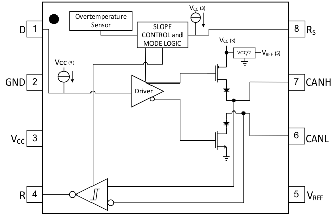
The HVD251 is intended for use in applications employing the Controller Area Network
(CAN) serial communication physical layer in accordance with the ISO 11898 Standard. The HVD251
provides differential transmit capability to the bus and differential receive capability to a CAN
controller at speeds up to 1 megabits per second (Mbps).Designed for operation in harsh environments, the device features cross-wire, overvoltage
and loss of ground protection to ±36 V. Also featured are overtemperature protection as well as
–7-V to 12-V common-mode range, and tolerance to transients of ±200 V. The transceiver interfaces
the single-ended CAN controller with the differential CAN bus found in industrial, building
automation, and automotive applications.Rs, pin 8, selects one of three different modes of operation: high-speed, slope control,
or low-power mode. The high-speed mode of operation is selected by connecting pin 8 to ground,
allowing the transmitter output transistors to switch as fast as possible with no limitation on the
rise and fall slope. The rise and fall slope can be adjusted by connecting a resistor to ground at
pin 8; the slope is proportional to the pin’s output current. Slope control with an external
resistor value of 10 kΩ gives about 15-V / µs slew rate; 100 kΩ gives about 2-V/µs slew rate.If a high logic level is applied to the Rs pin 8, the device enters a low-current standby
mode where the driver is switched off and the receiver remains active. The local protocol
controller returns the device to the normal mode when it transmits to the bus.
SN65HVD251DR 数据手册
SN65HVD251DR 电路图