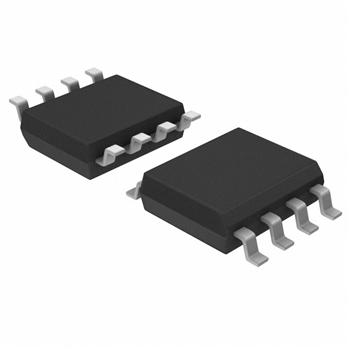
SN65HVD1794DR 供应商
-
SN65HVD1794DR
品牌:TI 封装/批号:原厂原装/22+ -
SN65HVD1794DR
品牌:TI/德州仪器 封装/批号:21+/SOP8 -
SN65HVD1794DR
品牌:TI(德州仪器) 封装/批号:SOIC-8/2022+ -
SN65HVD1794DR
品牌:TI 封装/批号:SOP/23+ -
SN65HVD1794DR
品牌:TI/德州仪器 封装/批号:/21+
SN65HVD1794DR 属性参数
- 标准包装:2,500
- 类别:集成电路 (IC)
- 家庭:接口 - 驱动器,接收器,收发器
- 系列:-
- 类型:收发器
- 驱动器/接收器数:1/1
- 规程:RS485
- 电源电压:4.5 V ~ 5.5 V
- 安装类型:表面贴装
- 封装/外壳:8-SOIC(0.154",3.90mm 宽)
- 供应商设备封装:8-SOIC
- 包装:带卷 (TR)
产品特性
- Bus-Pin Fault Protection to > ±70 V
- Cable Invert Function Allows Correction for Reversed Bus Pins
- Common-Mode Voltage Range (–20 V to 25 V) More Than Doubles TIA/EIA 485 Requirement
- Bus I/O Protection ±16 kV JEDEC HBM Protection
- ±16 kV JEDEC HBM Protection
- Reduced Unit Load for Up to 256 Nodes
- Failsafe Receiver for Open-Circuit, Short-Circuit and Idle-Bus Conditions
- Low Power Consumption ICC 5 mA Quiescent During Operation
- ICC 5 mA Quiescent During Operation
- Power-Up, Power-Down Glitch-Free Operation
产品概述
These devices are designed to survive overvoltage faults such as direct shorts to power
supplies, mis-wiring faults, connector failures, cable crushes, and tool mis-applications. They are
also robust to ESD events, with high levels of protection to human-body model specifications.These devices combine a differential driver and a differential receiver, which operate
from a single power supply. The driver differential outputs and the receiver differential inputs
are connected internally to for a bus port suitable for half-duplex (two-wire bus) communication. A
cable invert pin (INV) allows active correction of mis-wires that may occur during installation.
Upon detecting communication errors, the user can apply a logic HIGH to the INV pin, effectively
inverting the polarity of the differential bus port, thereby correcting for the reversed bus wires.These devices feature a wide common-mode voltage range, making them suitable for
multi-point applications over long cable runs. These devices are characterized from –40°C to 105°C.For similar features with 3.3 V supply operation, see the SN65HVD1781 (SLLS877).
