SN65HVD1040QDRQ1 供应商
-
SN65HVD1040QDRQ1
品牌:TI 封装/批号:原厂原装/22+ -
SN65HVD1040QDRQ1
品牌:TI 封装/批号:SO-8/09+ -
SN65HVD1040QDRQ1
品牌:TI/德州仪器 封装/批号:21+/SOP8 -
SN65HVD1040QDRQ1
品牌:TI(德州仪器) 封装/批号:SOIC-8_150mil/2022+ -
SN65HVD1040QDRQ1
品牌:SOP8 封装/批号:TI/22+ -
SN65HVD1040QDRQ1
品牌:TI 封装/批号:SOP/23+
SN65HVD1040QDRQ1 属性参数
- 标准包装:1
- 类别:集成电路 (IC)
- 家庭:接口 - 驱动器,接收器,收发器
- 系列:-
- 类型:收发器
- 驱动器/接收器数:1/1
- 规程:CAN
- 电源电压:4.75 V ~ 5.25 V
- 安装类型:表面贴装
- 封装/外壳:8-SOIC(0.154",3.90mm 宽)
- 供应商设备封装:8-SOIC
- 包装:®
- 其它名称:296-21592-6
产品特性
- Qualified for Automotive Applications
- AEC-Q100 Test Guidance With the Following: Device Temperature Grade 1: –40°C to 125°C Ambient Operating Temperature Device HBM ESD Classification Level: Level 3A for All Pins Except 1, 5, 6, and 7 Level 3B for Pins 1, 5, 6, and 7 Device CDM ESD Classification Level C6 Device MM ESD Classification Level M3
- Device Temperature Grade 1: –40°C to 125°C Ambient Operating Temperature
- Device HBM ESD Classification Level: Level 3A for All Pins Except 1, 5, 6, and 7 Level 3B for Pins 1, 5, 6, and 7
- Level 3A for All Pins Except 1, 5, 6, and 7
- Level 3B for Pins 1, 5, 6, and 7
- Device CDM ESD Classification Level C6
- Device MM ESD Classification Level M3
- Customer-Specific Configuration Control Can Be Supported Along With Major-Change Approval
- Improved Drop-In Replacement for TJA1040
- Meets or Exceeds the Requirements of ISO 11898-5
- GIFT/ICT Compliant
- ESD Protection up to ±8 kV (Human-Body Model) on Bus Pins
- Low-Current Standby Mode With Bus Wakeup, <12 µA Maximum
- High Electromagnetic Immunity (EMI)
- Low Electromagnetic Emissions (EME)
- Bus-Fault Protection of –27 V to 40 V
- Dominant Time-Out Function
- Thermal Shutdown Protection
- Power-Up or Down Glitch-Free Bus Inputs and Outputs High Input Impedance With Low VCC Monotonic Outputs During Power Cycling
- High Input Impedance With Low VCC
- Monotonic Outputs During Power Cycling
产品概述
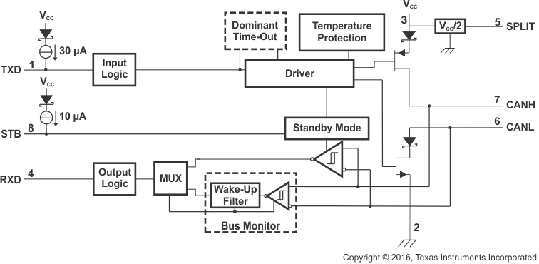
The SN65HVD1040-Q1 device meets or exceeds the specifications of the ISO 11898 standard
for use in applications employing a Controller Area Network (CAN). The device is qualified for use
in automotive applications.As a CAN transceiver, this device provides differential transmit capability to the bus
and differential receive capability to a CAN controller at signaling rates up to 1 megabit per
second (Mbps). The signaling rate of a line is the number of voltage transitions that are made per
second, expressed in the units bps (bits per second).Designed for operation in especially harsh environments, the SN65HVD1040-Q1 features
cross-wire, overvoltage, and loss of ground protection from –27 V to 40 V, overtemperature
protection, a –12-V to 12-V common-mode range, and withstands voltage transients from –200 V to 200
V, according to ISO 7637.STB (pin 8) provides two different modes of operation: high-speed mode or low-current
standby mode. The high-speed mode of operation is selected by connecting STB (pin 8) to ground.If a high logic level is applied to the STB pin of the SN65HVD1040-Q1, the device enters
a low-current standby mode, while the receiver remains active in a low-power bus-monitor standby
mode.In the low-current standby mode, a dominant bit greater than 5 µs on the bus is passed by
the bus-monitor circuit to the receiver output. The local protocol controller may then reactivate
the device when it needs to transmit to the bus.A dominant time-out circuit in the SN65HVD1040-Q1 prevents the driver from blocking
network communication with a hardware or software failure. The time-out circuit is triggered by a
falling edge on TXD (pin 1). If no rising edge is seen before the time-out constant of the circuit
expires, the driver is disabled. The circuit is then reset by the next rising edge on TXD.SPLIT (pin 5) is available as a VCC/2 common-mode bus voltage bias
for a split-termination network (see SPLIT).The SN65HVD1040 is characterized for operation from –40°C to 125°C.
SN65HVD1040QDRQ1 数据手册
SN65HVD1040QDRQ1 电路图