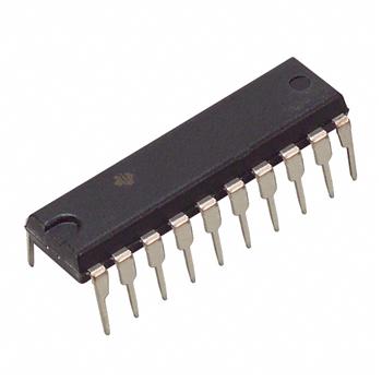
SN65C1154N 供应商
-
SN65C1154N
品牌:TI 封装/批号:原厂原装/22+ -
SN65C1154N
品牌:TI/德州仪器 封装/批号:21+/DIP20 -
SN65C1154N
品牌:TI 封装/批号:Quad Transmitter/Receiver RS-232 20-Pin PDIP Tub/22+
SN65C1154N 属性参数
- 标准包装:20
- 类别:集成电路 (IC)
- 家庭:接口 - 驱动器,接收器,收发器
- 系列:-
- 类型:线路收发器
- 驱动器/接收器数:4/4
- 规程:RS232
- 电源电压:4.5 V ~ 6 V
- 安装类型:通孔
- 封装/外壳:20-DIP(0.300",7.62mm)
- 供应商设备封装:20-PDIP
- 包装:管件
- 其它名称:296-11855-5
产品特性
- Meet or Exceed the Requirements of TIA/EIA-232-F and ITU Recommendation V.28
- Very Low Power Consumption . . .5 mW Typ
- Wide Driver Supply Voltage . . .±4.5 V to ±15 V
- Driver Output Slew Rate Limited to 30 V/µs Max
- Receiver Input Hysteresis . . . 1000 mV Typ
- Push-Pull Receiver Outputs
- On-Chip Receiver 1-µs Noise Filter
产品概述
The SN65C1164 and SN75C1154 are low-power BiMOS devices containing four independent drivers and receivers that are used to interface data terminal equipment (DTE) with data circuit-terminating equipment (DCE). These devices are designed to conform to TIA/EIA-232-F. The drivers and receivers of the SN65C1154 and SN75C1154 are similar to those of the SN75C188 quadruple driver and SN75C189A quadruple receiver, respectively. The drivers have a controlled output slew rate that is limited to a maximum of 30 V/µs and the receivers have filters that reject input noise pulses of shorter than 1 µs. Both these features eliminate the need for external components.The SN65C1154 and SN75C1154 have been designed using low-power techniques in a BiMOS technology. In most applications, the receivers contained in these devices interface to single inputs of peripheral devices such as ACEs, UARTs, or microprocessors. By using sampling, such peripheral devices usually are insensitive to the transition times of the input signals. If this is not the case, or for other uses, it is recommended that the SN65C1154 and SN75C1154 receiver outputs be buffered by single Schmitt input gates or single gates of the HCMOS, ALS, or 74F logic families.
