SM320F2812HFGM150 供应商
-
SM320F2812HFGM150
品牌:TI 封装/批号:CFPAK-172/21+ -
SM320F2812HFGM150
品牌:TI 封装/批号:CQFP/16+ -
SM320F2812HFGM150
品牌:TI 封装/批号:/最新批号
SM320F2812HFGM150 属性参数
- 制造商:Texas Instruments
- 产品种类:数字信号处理器与控制器 (DSP, DSC)
- 数据总线宽度:32 bit
- 程序存储器大小:1 K
- 数据 RAM 大小:36 KB
- 最大时钟频率:150 MHz
- 可编程输入/输出端数量:56
- 工作电源电压:1.9 V
- 最大工作温度:+ 125 C
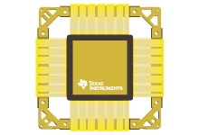
- 封装 / 箱体:CFP-172
- 安装风格:SMD/SMT
- 最小工作温度:- 55 C
- 产品:DSPs
- 程序存储器类型:OTP ROM
- 工厂包装数量:1
产品特性
- High-Performance Static CMOS Technology 150 MHz (6.67-ns Cycle Time) Low-Power (1.8-V Core at 135 MHz, 1.9-V Core at 150 MHz, 3.3-V I/O) Design 3.3-V Flash Voltage
- 150 MHz (6.67-ns Cycle Time)
- Low-Power (1.8-V Core at 135 MHz, 1.9-V Core at 150 MHz, 3.3-V I/O) Design
- 3.3-V Flash Voltage
- JTAG Boundary Scan Support
- High-Performance 32-Bit CPU (TMS320C28x) 16 x 16 and 32 x 32 MAC Operations 16 x 16 Dual MAC Harvard Bus Architecture Atomic Operations Fast Interrupt Response and Processing Unified Memory Programming Model 4M Linear Program Address Reach 4M Linear Data Address Reach Code-Efficient (in C/C++ and Assembly) TMS320F24x/LF240x Processor Source Code Compatible
- 16 x 16 and 32 x 32 MAC Operations
- 16 x 16 Dual MAC
- Harvard Bus Architecture
- Atomic Operations
- Fast Interrupt Response and Processing
- Unified Memory Programming Model
- 4M Linear Program Address Reach
- 4M Linear Data Address Reach
- Code-Efficient (in C/C++ and Assembly)
- TMS320F24x/LF240x Processor Source Code Compatible
- On-Chip Memory Flash Devices: Up to 128K x 16 Flash (Four 8K x 16 and Six 16K x 16 Sectors) ROM Devices: Up to 128K x 16 ROM 1K x 16 OTP ROM L0 and L1: 2 Blocks of 4K x 16 Each Single-Access RAM (SARAM) H0: 1 Block of 8K x 16 SARAM M0 and M1: 2 Blocks of 1K x 16 Each SARAM
- Flash Devices: Up to 128K x 16 Flash (Four 8K x 16 and Six 16K x 16 Sectors)
- ROM Devices: Up to 128K x 16 ROM
- 1K x 16 OTP ROM
- L0 and L1: 2 Blocks of 4K x 16 Each Single-Access RAM (SARAM)
- H0: 1 Block of 8K x 16 SARAM
- M0 and M1: 2 Blocks of 1K x 16 Each SARAM
- Boot ROM (4K x 16) With Software Boot Modes Standard Math Tables
- With Software Boot Modes
- Standard Math Tables
- External Interface Up to 1M Total Memory Programmable Wait States Programmable Read/Write Strobe Timing Three Individual Chip Selects
- Up to 1M Total Memory
- Programmable Wait States
- Programmable Read/Write Strobe Timing
- Three Individual Chip Selects
- Clock and System Control Dynamic PLL Ratio Changes Supported On-Chip Oscillator Watchdog Timer Module
- Dynamic PLL Ratio Changes Supported
- On-Chip Oscillator
- Watchdog Timer Module
- Three External Interrupts
- Peripheral Interrupt Expansion (PIE) Block That Supports 45 Peripheral Interrupts
- 128-Bit Security Key/Lock Protects Flash/ROM/OTP and L0/L1 SARAM Prevents Firmware Reverse Engineering
- Protects Flash/ROM/OTP and L0/L1 SARAM
- Prevents Firmware Reverse Engineering
- Three 32-Bit CPU-Timers
- Motor Control Peripherals Two Event Managers (EVA, EVB) Compatible to 240xA Devices
- Two Event Managers (EVA, EVB)
- Compatible to 240xA Devices
- Serial Port Peripherals Serial Peripheral Interface (SPI) Two Serial Communications Interfaces (SCIs), Standard UART Enhanced Controller Area Network (eCAN) Multichannel Buffered Serial Port (McBSP) With SPI Mode
- Serial Peripheral Interface (SPI)
- Two Serial Communications Interfaces (SCIs), Standard UART
- Enhanced Controller Area Network (eCAN)
- Multichannel Buffered Serial Port (McBSP) With SPI Mode
- 12-Bit ADC, 16 Channels 2 x 8 Channel Input Multiplexer Two Sample-and-Hold Single/Simultaneous Conversions Fast Conversion Rate: 80 ns/12.5 MSPS
- 2 x 8 Channel Input Multiplexer
- Two Sample-and-Hold
- Single/Simultaneous Conversions
- Fast Conversion Rate: 80 ns/12.5 MSPS
- Up to 56 Individually Programmable, Multiplexed General-Purpose Input/Output (GPIO) Pins
- Advanced Emulation Features Analysis and Breakpoint Functions Real-Time Debug via Hardware
- Analysis and Breakpoint Functions
- Real-Time Debug via Hardware
- Development Tools Include ANSI C/C++ Compiler/Assembler/Linker Supports TMS320C24x™/240x Instructions Code Composer Studio™ IDE DSP/BIOS™ JTAG Scan Controllers [Texas Instruments (TI) or Third-Party] Evaluation Modules Broad Third-Party Digital Motor Control Support
- ANSI C/C++ Compiler/Assembler/Linker
- Supports TMS320C24x™/240x Instructions
- Code Composer Studio™ IDE
- DSP/BIOS™
- JTAG Scan Controllers [Texas Instruments (TI) or Third-Party]
- Evaluation Modules
- Broad Third-Party Digital Motor Control Support
- Low-Power Modes and Power Savings IDLE, STANDBY, HALT Modes Supported Disable Individual Peripheral Clocks
- IDLE, STANDBY, HALT Modes Supported
- Disable Individual Peripheral Clocks
- Package Options 172-Pin Ceramic Quad Flatpack (HFG)
- 172-Pin Ceramic Quad Flatpack (HFG)
- Temperature Options: M: –55°C to 125°C (HFG)
- M: –55°C to 125°C (HFG)
产品概述
The SM320F2812 device, member of the C28x™ DSP generation, is a highly integrated, high-performance solution for demanding control applications. The functional blocks and the memory maps are described in Section 3, Functional Overview.Throughout this document, SM320F2812 is abbreviated as F2812.
SM320F2812HFGM150 电路图