SCAN90CP02SP 供应商
-
SCAN90CP02SP/NOPB
品牌:TI 封装/批号:原厂原装/22+
SCAN90CP02SP 属性参数
- 制造商:National Semiconductor (TI)
- 封装:Reel
- 工厂包装数量:1000
产品特性
- 1.5 Gbps per Channel
- Low Power: 70 mA in Dual Repeater Mode @1.5 Gbps
- Low Output Jitter
- Configurable 0/25/50/100% Pre-Emphasis Drives Lossy Backplanes and Cables
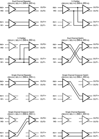
- Non-Blocking Architecture Allows 1:2 Splitter, 2:1 Mux, Crossover, and Dual Buffer Configurations
- Flow-Through Pinout
- LVDS/BLVDS/CML/LVPECL Inputs, LVDS Outputs
- IEEE 1149.1 and 1149.6 Compliant
- Single 3.3V Supply
- Separate Control of Inputs and Outputs Allows for Power Savings
- Industrial -40 to +85°C Temperature Range
- 28-Lead UQFN Package, or 32-Lead LQFP Package
产品概述
The SCAN90CP02 is a 1.5 Gbps 2 x 2 LVDS crosspoint switch. High speed data paths and
flow-through pinout minimize internal device jitter, while configurable 0/25/50/100% pre-emphasis
overcomes external ISI jitter effects of lossy backplanes and cables. The differential inputs
interface to LVDS and Bus LVDS signals such as those on TI's 10-, 16-, and 18- bit Bus LVDS SerDes,
as well as CML and LVPECL. The SCAN90CP02 can also be used with ASICs and FPGAs. The non-blocking
crosspoint architecture is pin-configurable as a 1:2 clock or data splitter, 2:1 redundancy mux,
crossover function, or dual buffer for signal booster and stub hider applications.Integrated IEEE 1149.1 (JTAG) and 1149.6 circuitry supports testability of both
single-ended LVTTL/CMOS and differential LVDS PCB interconnect. The 3.3V supply, CMOS process, and
LVDS I/O ensure high performance at low power over the entire industrial -40 to +85°C temperature
range.
SCAN90CP02SP 数据手册
SCAN90CP02SP 电路图
