LM5112MY/NOPB 供应商
-
LM5112MY/NOPB
品牌:TI 封装/批号:原厂原装/22+ -
LM5112MY/NOPB
品牌:TI(德州仪器) 封装/批号:MSOP-8/2022+
LM5112MY/NOPB 属性参数
- 制造商:National Semiconductor (TI)
- 类型:Low Side
- 上升时间:14 ns (Typ)
- 下降时间:12 ns (Typ)
- Supply Voltage - Max:14 V
- Supply Voltage - Min:3.5 V
- 电源电流:2 mA
- 最大工作温度:+ 125 C
- 安装风格:SMD/SMT
- 封装 / 箱体:MSOP
- 封装:Reel
- 配置:Inverting, Non-Inverting
- 最小工作温度:- 40 C
- 激励器数量:1
- 输出端数量:1
- 输出电流:7 A (Typ)
- 工厂包装数量:1000
产品特性
- LM5112-Q1 is Qualified for Automotive Applications
- AEC-Q100 Grade 1 Qualified
- Manufactured on an Automotive Grade Flow
- Compound CMOS and Bipolar Outputs Reduce Output Current Variation
- 7-A Sink and 3-A Source Current
- Fast Propagation Times: 25 ns (Typical)
- Fast Rise and Fall Times: 14 ns or 12 ns Rise or Fall With 2-nF Load
- Inverting and Non-Inverting Inputs Provide Either Configuration With a Single Device
- Supply Rail Undervoltage Lockout Protection
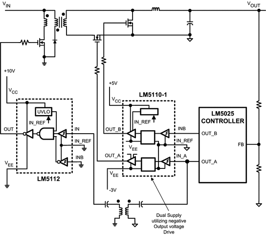
- Dedicated Input Ground (IN_REF) for Split Supply or Single Supply Operation
- Power Enhanced 6-Pin WSON Package (3 mm × 3 mm) or Thermally Enhanced MSOP-PowerPAD Package
- Output Swings From VCC to VEE Which Are Negative Relative to Input Ground
产品概述
The LM5112 device MOSFET gate driver provides high peak gate drive current in the tiny
6-pin WSON package (SOT-23 equivalent footprint) or an 8-pin exposed-pad MSOP package with improved
power dissipation required for high frequency operation. The compound output driver stage includes
MOS and bipolar transistors operating in parallel that together sink more than 7 A peak from
capacitive loads. Combining the unique characteristics of MOS and bipolar devices reduces drive
current variation with voltage and temperature. Undervoltage lockout protection is provided to
prevent damage to the MOSFET due to insufficient gate turnon voltage. The LM5112 device provides
both inverting and non-inverting inputs to satisfy requirements for inverting and non-inverting
gate drive with a single device type.
LM5112MY/NOPB 电路图