LF356N 供应商
LF356N 属性参数
- 制造商:National Semiconductor (TI)
- 通道数量:1
- 共模抑制比(最小值):80 dB
- 输入补偿电压:10 mV at +/- 15 V
- 安装风格:Through Hole
- 封装 / 箱体:MDIP
- 转换速度:12 V/us at +/- 15 V
- 关闭:No
- 最大工作温度:+ 70 C
- 封装:Tube
- 最小工作温度:0 C
- 工厂包装数量:40
- 电源电流:10 mA at +/- 15 V
- 技术:BiFET
- 电压增益 dB:106.02 dB
产品特性
- Advantages Replace Expensive Hybrid and Module FET Op Amps Rugged JFETs Allow Blow-Out Free Handling Compared With MOSFET Input Devices Excellent for Low Noise Applications Using Either High or Low Source Impedance–Very Low 1/f Corner Offset Adjust Does Not Degrade Drift or Common-Mode Rejection as in Most Monolithic Amplifiers New Output Stage Allows Use of Large Capacitive Loads (5,000 pF) Without Stability Problems Internal Compensation and Large Differential Input Voltage Capability
- Replace Expensive Hybrid and Module FET Op Amps
- Rugged JFETs Allow Blow-Out Free Handling Compared With MOSFET Input Devices
- Excellent for Low Noise Applications Using Either High or Low Source Impedance–Very Low 1/f Corner
- Offset Adjust Does Not Degrade Drift or Common-Mode Rejection as in Most Monolithic Amplifiers
- New Output Stage Allows Use of Large Capacitive Loads (5,000 pF) Without Stability Problems
- Internal Compensation and Large Differential Input Voltage Capability
- Common Features Low Input Bias Current: 30 pA Low Input Offset Current: 3 pA High Input Impedance: 1012 Ω Low Input Noise Current: 0.01 pA/√Hz High Common-Mode Rejection Ratio: 100 dB Large DC Voltage Gain: 106 dB
- Low Input Bias Current: 30 pA
- Low Input Offset Current: 3 pA
- High Input Impedance: 1012 Ω
- Low Input Noise Current: 0.01 pA/√Hz
- High Common-Mode Rejection Ratio: 100 dB
- Large DC Voltage Gain: 106 dB
- Uncommon Features Extremely Fast Settling Time to 0.01%: 4 µs for the LFx55 devices 1.5 µs for the LFx56 1.5 µs for the LFx57 (AV = 5) Fast Slew Rate: 5 V/µs for the LFx55 12 V/µs for the LFx56 50 V/µs for the LFx57 (AV = 5) Wide Gain Bandwidth: 2.5 MHz for the LFx55 devices 5 MHz for the LFx56 20 MHz for the LFx57 (AV = 5) Low Input Noise Voltage: 20 nV/√Hz for the LFx55 12 nV/√Hz for the LFx56 12 nV/√Hz for the LFx57 (AV = 5)
- Extremely Fast Settling Time to 0.01%: 4 µs for the LFx55 devices 1.5 µs for the LFx56 1.5 µs for the LFx57 (AV = 5)
- 4 µs for the LFx55 devices
- 1.5 µs for the LFx56
- 1.5 µs for the LFx57 (AV = 5)
- Fast Slew Rate: 5 V/µs for the LFx55 12 V/µs for the LFx56 50 V/µs for the LFx57 (AV = 5)
- 5 V/µs for the LFx55
- 12 V/µs for the LFx56
- 50 V/µs for the LFx57 (AV = 5)
- Wide Gain Bandwidth: 2.5 MHz for the LFx55 devices 5 MHz for the LFx56 20 MHz for the LFx57 (AV = 5)
- 2.5 MHz for the LFx55 devices
- 5 MHz for the LFx56
- 20 MHz for the LFx57 (AV = 5)
- Low Input Noise Voltage: 20 nV/√Hz for the LFx55 12 nV/√Hz for the LFx56 12 nV/√Hz for the LFx57 (AV = 5)
- 20 nV/√Hz for the LFx55
- 12 nV/√Hz for the LFx56
- 12 nV/√Hz for the LFx57 (AV = 5)
产品概述
The LFx5x devices are the first monolithic JFET input operational amplifiers to
incorporate well-matched, high-voltage JFETs on the same chip with standard bipolar transistors
(BI-FET™ Technology). These amplifiers feature low
input bias and offset currents/low offset voltage and offset voltage drift, coupled with offset
adjust, which does not degrade drift or common-mode rejection. The devices are also designed for
high slew rate, wide bandwidth, extremely fast settling time, low voltage and current noise and a
low 1/f noise corner.
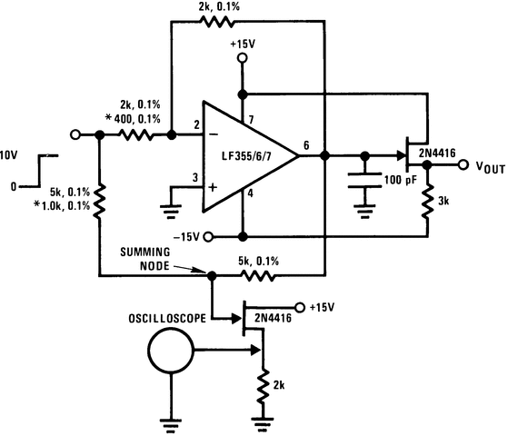
LF356N 电路图