DS92LX1621SQE/NOPB 供应商
-
DS92LX1621SQE/NOPB
品牌:TI 封装/批号:原厂原装/22+ -
DS92LX1621SQE/NOPB
品牌:TI(德州仪器) 封装/批号:WQFN-32(5x5)/2022+ -
DS92LX1621SQE/NOPB
品牌:TI 封装/批号:原厂原封装/新批号
DS92LX1621SQE/NOPB 属性参数
- 制造商:National Semiconductor (TI)
- 数据速率:16 bit
- 最大工作温度:+ 85 C
- 最小工作温度:- 40 C
- 工作电源电压:1.8 V, 3.3 V
- 封装 / 箱体:LLP-32
- 安装风格:SMD/SMT
- 输出端数量:2
- 工作电流:1 uA
- 封装:Reel
- 工厂包装数量:250
- Supply Voltage - Max:1.89 V, 3.6 V
- Supply Voltage - Min:1.71 V, 3 V
- 类型:Network Controller & Processor
产品特性
- Configurable Data Throughput 12–bit (min) up to 600 Mbits/sec 16–bit (def) up to 800 Mbits/sec 18–bit (max) up to 900 Mbits/sec
- 12–bit (min) up to 600 Mbits/sec
- 16–bit (def) up to 800 Mbits/sec
- 18–bit (max) up to 900 Mbits/sec
- 10 MHz to 50 MHz Input Clock Support
- Embedded Clock with DC Balanced Coding to Support AC-Coupled Interconnects
- Capable to Drive up to 10 Meters Shielded Twisted-Pair
- Bi-Directional Control Interface Channel with I2C Support
- I2C Interface for Device Configuration. Single-pin ID Addressing
- 16–bit Data Payload with CRC (Cyclic Redundancy Check) for Checking Data Integrity with Programmable Data Transmission Error Detection and Interrupt Control
- Up to 6 Programmable GPIO’s
- AT-SPEED BIST Diagnosis Feature to Validate Link Integrity
- Individual Power-Down Controls for Both SER and DES
- User-Selectable Clock Edge for Parallel Data on Both SER and DES
- Integrated Termination Resistors
- 1.8V- or 3.3V-Compatible Parallel Bus Interface
- Single Power Supply at 1.8V
- IEC 61000–4–2 ESD Compliant
- No Reference Clock Required on Deserializer
- Programmable Receive Equalization
- LOCK Output Reporting Pin to Ensure Link Status
- EMI/EMC Mitigation DES Programmable Spread Spectrum (SSCG) Outputs DES Receiver Staggered Outputs
- DES Programmable Spread Spectrum (SSCG) Outputs
- DES Receiver Staggered Outputs
- Temperature Range −40°C to +85°C
- SER Package: 32 Pin WQFN (5mm × 5mm)
- DES Package: 40 Pin WQFN (6mm × 6mm)
产品概述
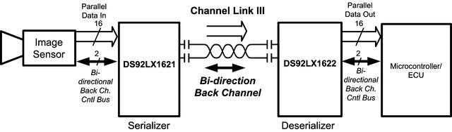
The DS92LX1621 / DS92LX1622 chipset offers a Channel Link III interface with a high-speed
forward channel and a full-duplex back channel for data transmission over a single differential
pair. The Serializer/Deserializer pair is targeted for direct connections between automotive camera
systems and Host Controller/Electronic Control Unit (ECU). The primary transport sends 16 bits of
image data over a single high-speed serial stream together with a low latency bi-directional
control channel transport that supports I2C. Included with the 16-bit
payload is a selectable data integrity option for CRC (Cyclic Redundancy Check) or parity bit to
monitor transmission link errors. Using TI’s embedded clock technology allows transparent
full-duplex communication over a single differential pair, carrying asymmetrical bi-directional
control information without the dependency of video blanking intervals. This single serial stream
simplifies transferring a wide data bus over PCB traces and cable by eliminating the skew problems
between parallel data and clock paths. This significantly saves system cost by narrowing data paths
that in turn reduce PCB layers, cable width, and connector size and pins.In addition, the Deserializer inputs provide equalization control to compensate for loss
from the media over longer distances. Internal DC balanced encoding/decoding is used to support
AC-Coupled interconnects.The sleep function provides a power-savings mode and a remote wake up interrupt for
signaling of a remote device.The Serializer is offered in a 32-pin WQFN package, and Deserializer is offered in a
40-pin WQFN package.
DS92LX1621SQE/NOPB 数据手册
DS92LX1621SQE/NOPB 电路图