DS90LV110TMTCX 供应商
-
DS90LV110TMTCX
品牌:TI 封装/批号:原厂原装/22+ -
DS90LV110TMTCX
品牌:NS 封装/批号:SOP-8/23+ -
DS90LV110TMTCX
品牌:NS 封装/批号:TSSOP-28/23+ -
DS90LV110TMTCX
品牌:NSC/ELNAF 封装/批号:TSSOP-2/1926+ -
DS90LV110TMTCX/NOPB
品牌:TI(德州仪器) 封装/批号:TSSOP-28/2022+ -
DS90LV110TMTCX+
品牌:TI/NS 封装/批号:/21+
DS90LV110TMTCX 属性参数
- 制造商:National Semiconductor (TI)
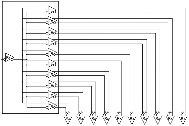
- 激励器数量:10
- 接收机数量:1
- 数据速率:400 Mbps
- 工作电源电压:3.3 V
- 最大功率耗散:413 mW (Typ)
- 最大工作温度:+ 85 C
- 封装 / 箱体:TSSOP-28
- 封装:Reel
- 最小工作温度:- 40 C
- 安装风格:SMD/SMT
- 传播延迟时间:3.6 ns
- 工厂包装数量:2500
- Supply Voltage - Max:3.6 V
- Supply Voltage - Min:3 V
- 类型:LVDS
产品特性
- Low jitter 800 Mbps fully differential data path
- 145 ps (typ) of pk-pk jitter with PRBS = 223−1 data pattern at 800 Mbps
- Single +3.3 V Supply
- Less than 413 mW (typ) total power dissipation
- Balanced output impedance
- Output channel-to-channel skew is 35ps (typ)
- Differential output voltage (VOD) is 320mV (typ) with 100Ω termination load.
- LVDS receiver inputs accept LVPECL signals
- Fast propagation delay of 2.8 ns (typ)
- Receiver input threshold < ±100 mV
- 28 lead TSSOP package
- Conforms to ANSI/TIA/EIA-644 LVDS standard
产品概述
DS90LV110 is a 1 to 10 data/clock
distributor utilizing LVDS (Low Voltage Differential Signaling) technology for low power, high
speed operation. Data paths are fully differential from input to output for low noise generation
and low pulse width distortion. The design allows connection of 1 input to all 10 outputs. LVDS I/O
enable high speed data transmission for point-to-point interconnects. This device can be used as a
high speed differential 1 to 10 signal distribution / fanout replacing multi-drop bus applications
for higher speed links with improved signal quality. It can also be used for clock distribution up
to 400MHz.The DS90LV110 accepts LVDS signal levels, LVPECL levels directly or PECL with attenuation
networks. The LVDS outputs can be put into TRI-STATE by use of the enable pin.For more details, please refer to the Application Information section of this datasheet.
DS90LV110TMTCX 电路图