DS90LV019TM/NOPB 供应商
-
DS90LV019TM/NOPB
品牌:TI 封装/批号:原厂原装/22+ -
DS90LV019TM/NOPB
品牌:TI(德州仪器) 封装/批号:SOIC-14/2022+
DS90LV019TM/NOPB 属性参数
- 制造商:National Semiconductor (TI)
- 激励器数量:2
- 接收机数量:2
- 数据速率:100 Mbps
- 工作电源电压:3.3 V
- 最大功率耗散:960 mW
- 最大工作温度:+ 85 C
- 封装 / 箱体:SOIC-14
- 封装:Tube
- 最小工作温度:- 40 C
- 安装风格:SMD/SMT
- 传播延迟时间:7 ns
- 工厂包装数量:55
- Supply Voltage - Max:3.6 V
- Supply Voltage - Min:3 V
- 类型:LVCMOS, LVTTL, LVDS
产品特性
- LVDS Signaling
- 3.3V or 5.0V operation
- Low power CMOS design
- Balanced Output Impedance
- Glitch free power up/down (Driver disabled)
- High Signaling Rate Capacity (above 100 Mbps)
- Ultra Low Power Dissipation
- ±1V Common-Mode Range
- ±100 mV Receiver Sensitivity
- Product offered in SOIC and TSSOP packages
- Flow-Through Pin Out
- Industrial Temperature Range Operation
产品概述
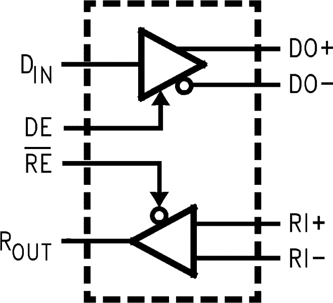
The DS90LV019 is a Driver/Receiver designed specifically for the high speed low power point-to-point interconnect applications. The device operates from a single 3.3V or 5.0V power supply and includes one differential line driver and one receiver. The DS90LV019 features an independent driver and receiver with TTL/CMOS compatibility (DIN and ROUT). The logic interface provides maximum flexibility as 4 separate lines are provided (DIN, DE, RE#, and ROUT). The device also features a flow-through pin out which allows easy PCB routing for short stubs between its pins and the connector. The driver has 3.5 mA output loop current.The driver translates between TTL levels (single-ended) to Low Voltage Differential Signaling levels. This allows for high speed operation, while consuming minimal power with reduced EMI. In addition, the differential signaling provides common-mode noise rejection.The receiver threshold is ±100 mV over a ±1V common-mode range and translates the low swing differential levels to standard (TTL/CMOS) levels.
DS90LV019TM/NOPB 数据手册
DS90LV019TM/NOPB 电路图