DS90LV001TLDX 供应商
-
DS90LV001TLDX
品牌:TI 封装/批号:原厂原装/22+ -
DS90LV001TLDX
品牌:NSC 封装/批号:LLP/4
DS90LV001TLDX 属性参数
- 制造商:National Semiconductor (TI)
- 激励器数量:1
- 接收机数量:1
- 数据速率:800 Mbps
- 工作电源电压:3.3 V
- 最大功率耗散:726 mW
- 最大工作温度:+ 85 C
- 封装 / 箱体:LLP EP
- 封装:Reel
- 最小工作温度:- 40 C
- 传播延迟时间:2 ns
- 工厂包装数量:4500
- Supply Voltage - Max:3.6 V
- Supply Voltage - Min:3 V
- 类型:LVDS
产品特性
- Single +3.3 V Supply
- LVDS Receiver Inputs Accept LVPECL Signals
- TRI-STATE Outputs
- Receiver Input Threshold < ±100 mV
- Fast Propagation Delay of 1.4 ns (Typ)
- Low Jitter 800 Mbps Fully Differential Data Path
- 100 ps (Typ) of pk-pk Jitter with PRBS = 223−1 Data Pattern at 800 Mbps
- Compatible with ANSI/TIA/EIA-644-A LVDS Standard
- 8 pin SOIC and Space Saving (70%) WSON Package
- Industrial Temperature Range
产品概述
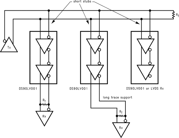
The DS90LV001 LVDS-LVDS Buffer takes an LVDS input signal and provides an LVDS output
signal. In many large systems, signals are distributed across backplanes, and one of the limiting
factors for system speed is the "stub length" or the distance between the transmission line and the
unterminated receivers on individual cards. Although it is generally recognized that this distance
should be as short as possible to maximize system performance, real-world packaging concerns often
make it difficult to make the stubs as short as the designer would like.The DS90LV001, available in the WSON package, will allow the receiver to be placed very
close to the main transmission line, thus improving system performance.A wide input dynamic range will allow the DS90LV001 to receive differential signals from
LVPECL as well as LVDS sources. This will allow the device to also fill the role of an LVPECL-LVDS
translator.An output enable pin is provided, which allows the user to place the LVDS output in
TRI-STATE.The DS90LV001 is offered in two package options, an 8 pin WSON and SOIC.
DS90LV001TLDX 电路图