DS90CR484AVJD/NOPB 供应商
-
DS90CR484AVJD/NOPB
品牌:TI 封装/批号:原厂原装/22+ -
DS90CR484AVJD/NOPB
品牌:TI(德州仪器) 封装/批号:TQFP-100(14x14)/2022+
DS90CR484AVJD/NOPB 属性参数
- 制造商:National Semiconductor (TI)
- 激励器数量:48
- 接收机数量:8
- 数据速率:672 Mbps
- 工作电源电压:3.3 V
- 最大功率耗散:2300 mW
- 最大工作温度:+ 70 C
- 封装 / 箱体:TQFP-100
- 封装:Tray
- 最小工作温度:- 10 C
- 安装风格:SMD/SMT
- 工厂包装数量:90
- Supply Voltage - Max:3.6 V
- Supply Voltage - Min:3 V
- 类型:CMOS, TTL
产品特性
- Up to 5.38 Gbits/sec Bandwidth
- 33 MHz to 112 MHz Input Clock Support
- LVDS SER/DES Reduces Cable and Connector Size
- Pre-emphasis Reduces Cable Loading Effects
- DC Balance Data Transmission Provided by Transmitter Reduces ISI Distortion
- Cable Deskew of +/−1 LVDS Data Bit Time (up to 80 MHz Clock Rate)
- 5V Tolerant TxIN and Control Input Pins
- Flow Through Pinout for Easy PCB Design
- +3.3V Supply Voltage
- Transmitter Rejects Cycle-to-Cycle Jitter
- Conforms to ANSI/TIA/EIA-644-1995 LVDS Standard
- Both Devices are Available in 100 Lead TQFP Package
产品概述
The DS90CR483A transmitter converts 48 bits of CMOS/TTL data into
eight LVDS (Low Voltage Differential Signaling) data streams. A phase-locked transmit clock is
transmitted in parallel with the data streams over a ninth LVDS link. Every cycle of the transmit
clock 48 bits of input data are sampled and transmitted. The DS90CR484A receiver converts the LVDS
data streams back into 48 bits of CMOS/TTL data. At a transmit clock frequency of 112MHz, 48 bits
of TTL data are transmitted at a rate of 672Mbps per LVDS data channel. Using a 112MHz clock, the
data throughput is 5.38Gbit/s (672Mbytes/s).The multiplexing of data lines provides a substantial cable reduction.
Long distance parallel single-ended buses typically require a ground wire per active signal (and
have very limited noise rejection capability). Thus, for a 48-bit wide data and one clock, up to 98
conductors are required. With this Channel Link chipset as few as 19 conductors (8 data pairs, 1
clock pair and a minimum of one ground) are needed. This provides an 80% reduction in cable width,
which provides a system cost savings, reduces connector physical size and cost, and reduces
shielding requirements due to the cables' smaller form factor.The 48 CMOS/TTL inputs can support a variety of signal combinations. For example, 6 8-bit
words or 5 9-bit (byte + parity) and 3 controls.The DS90CR483A/DS90CR484A chipset is improved over prior generations of Channel Link
devices and offers higher bandwidth support and longer cable drive with three areas of enhancement.
To increase bandwidth, the maximum clock rate is increased to 112 MHz and 8 serialized LVDS outputs
are provided. Cable drive is enhanced with a user selectable pre-emphasis feature that provides
additional output current during transitions to counteract cable loading effects. Optional DC
balancing on a cycle-to-cycle basis, is also provided to reduce ISI (Inter-Symbol Interference).
With pre-emphasis and DC balancing, a low distortion eye-pattern is provided at the receiver end of
the cable. A cable deskew capability has been added to deskew long cables of pair-to-pair skew of
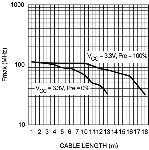
up to +/−1 LVDS data bit time (up to 80 MHz Clock Rate). These three enhancements allow cables 5+
meters in length to be driven.The chipset is an ideal means to solve EMI and cable size problems associated with wide,
high speed TTL interfaces.For more details, please refer to the section of this datasheet.
DS90CR484AVJD/NOPB 数据手册
DS90CR484AVJD/NOPB 电路图