DAC8812ICPWG4 供应商
-
DAC8812ICPWG4
品牌:TI 封装/批号:原厂原装/22+ -
DAC8812ICPWG4
品牌:TI(德州仪器) 封装/批号:TSSOP-16/2022+
DAC8812ICPWG4 属性参数
- 产品培训模块:Data Converter Basics
- 标准包装:90
- 类别:集成电路 (IC)
- 家庭:数据采集 - 数模转换器
- 系列:-
- 设置时间:300ns
- 位数:16
- 数据接口:串行
- 转换器数目:2
- 电压电源:单电源
- 功率耗散(最大):25µW
- 工作温度:-40°C ~ 85°C
- 安装类型:表面贴装
- 封装/外壳:16-TSSOP(0.173",4.40mm 宽)
- 供应商设备封装:16-TSSOP
- 包装:管件
- 输出数目和类型:2 电流,单极;2 电流,双极
- 采样率(每秒):2M
产品特性
- Relative Accuracy: 1 LSB Max
- Differential Nonlinearity: 1 LSB Max
- 2-mA Full-Scale Current ±20%, With VREF = ±10 V
- 0.5-μs Settling Time
- Midscale or Zero-Scale Reset
- Separate 4Q Multiplying Reference Inputs
- Reference Bandwidth: 10 MHz
- Reference Dynamics: –105-dB THD
- SPI-Compatible 3-Wire Interface: 50 MHz
- Double Buffered Registers to Enable Simultaneous Multichannel Update
- Internal Power-On Reset
- Industry-Standard Pin Configuration
产品概述
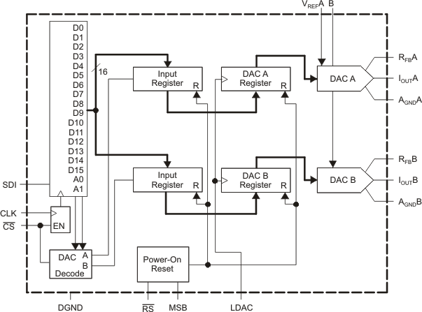
The DAC8812 is a dual, 16-bit, current-output digital-to-analog converter (DAC) designed
to operate from a single 2.7-V to 5.5-V supply.The applied external reference input voltage VREF determines the
full-scale output current. An internal feedback resistor (RFB) provides
temperature tracking for the full-scale output when combined with an external I-to-V precision
amplifier.A double-buffered, serial data interface offers high-speed, 3-wire, SPI and
microcontroller compatible inputs using serial data in (SDI), clock (CLK), and a chip-select
(CS). A common level-sensitive load DAC strobe (LDAC)
input allows simultaneous update of all DAC outputs from previously loaded input registers.
Additionally, an internal power-on reset forces the output voltage to zero at system turnon. An MSB
pin allows system reset assertion (RS) to force all registers to zero code
when MSB = 0, or to midscale code when MSB = 1.
DAC8812ICPWG4 电路图