DAC8555IPW 供应商
-
DAC8555IPW
品牌:TI 封装/批号:原厂原装/22+ -
DAC8555IPW
品牌:BB 封装/批号:UNKNOWN/7 -
DAC8555IPW
品牌:TI 封装/批号:16TSSOP/2019+ -
DAC8555IPW
品牌:TI(德州仪器) 封装/批号:TSSOP-16/2022+ -
DAC8555IPW
品牌:BB 封装/批号:SMD/23+ -
DAC8555IPW
品牌:TI 封装/批号:原厂原封装/新批号 -
DAC8555IPW
品牌:TI 封装/批号:16TSSOP/23+
DAC8555IPW 属性参数
- 产品培训模块:Data Converter Basics
- 标准包装:90
- 类别:集成电路 (IC)
- 家庭:数据采集 - 数模转换器
- 系列:-
- 设置时间:8µs
- 位数:16
- 数据接口:串行
- 转换器数目:4
- 电压电源:单电源
- 功率耗散(最大):3mW
- 工作温度:-40°C ~ 105°C
- 安装类型:表面贴装
- 封装/外壳:16-TSSOP(0.173",4.40mm 宽)
- 供应商设备封装:16-TSSOP
- 包装:管件
- 输出数目和类型:4 电压,单极;4 电压,双极
- 采样率(每秒):200k
- 配用:DAC8555EVM-ND - DAC8555EVM
- 其它名称:296-19402-5
产品特性
- Relative Accuracy: 4LSB
- Glitch Energy: 0.15nV-s
- MicroPower Operation: 150µA per Channel at 2.7V
- Power-On Reset to Zero-Scale or Midscale
- Power Supply: +2.7V to +5.5V
- 16-Bit Monotonic Over Temperature
- Settling Time: 10µs to ±0.003% FSR
- Ultra-Low AC Crosstalk: -100dB Typ
- Low-Power SPI-Compatible Serial Interface with Schmitt-Triggered Inputs: Up to 50MHz
- On-Chip Output Buffer Amplifier with Rail-to-Rail Operation
- Double Buffered Input Architecture
- Simultaneous or Sequential Output Update and Power-Down
- Binary and 2's Complement Capability
- Asynchronous Clear to Zero-Scale and Midscale
- 1.8V to 5.5V Logic Compatibility
- Available in a TSSOP-16 Package
- APPLICATIONSPortable InstrumentationClosed-Loop Servo-ControlProcess ControlData Acquisition SystemsProgrammable AttenuationPC Peripherals
- Portable Instrumentation
- Closed-Loop Servo-Control
- Process Control
- Data Acquisition Systems
- Programmable Attenuation
- PC Peripherals
产品概述
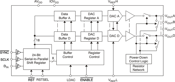
The DAC8555 is a 16-bit, quad channel, voltage output digital-to-analog converter (DAC) offering low-power operation and a flexible serial host interface. It offers monotonicity, good linearity, and exceptionally low glitch. Each on-chip precision output amplifier allows rail-to-rail output swing to be achieved over the supply range of 2.7V to 5.5V. The device supports a standard 3-wire serial interface capable of operating with input data clock frequencies up to 50MHz for IOVDD = 5V.The DAC8555 requires an external reference voltage to set the output range of each DAC channel. Also incorporated into the device is a power-on reset circuit, which can be programmed to ensure that the DAC outputs power up at zero-scale or midscale and remain there until a valid write takes place. The device also has the capability to function in both binary and 2's complement mode. The DAC8555 provides a per channel power-down feature, accessed over the serial interface, that reduces the current consumption to 175nA per channel at 5V.The low-power consumption of this device in normal operation makes it ideally suited to portable battery- operated equipment and other low-power applications. The power consumption is 5mW at 5V, reducing to 4µW in power-down mode.The DAC8555 is available in a TSSOP-16 package with a specified operating temperature range of -40°C to +105°C.
DAC8555IPW 电路图