CDCVF2505PWRG4 供应商
-
CDCVF2505PWRG4
品牌:TI 封装/批号:原厂原装/22+
CDCVF2505PWRG4 属性参数
- 标准包装:2,000
- 类别:集成电路 (IC)
- 家庭:时钟/计时 - 时钟发生器,PLL,频率合成器
- 系列:-
- 类型:PLL 时钟驱动器
- PLL:带旁路
- 输入:LVTTL
- 输出:LVTTL
- 电路数:1
- 比率 - 输入:输出:1:5
- 差分 - 输入:输出:无/无
- 频率 - 最大:200MHz
- 除法器/乘法器:无/无
- 电源电压:3 V ~ 3.6 V
- 工作温度:-40°C ~ 85°C
- 安装类型:表面贴装
- 封装/外壳:8-TSSOP(0.173",4.40mm 宽)
- 供应商设备封装:8-TSSOP
- 包装:带卷 (TR)
产品特性
- Phase-Lock Loop Clock Driver for Synchronous DRAM and General-Purpose Applications
- Spread Spectrum Clock Compatible
- Operating Frequency: 24 MHz to 200 MHz
- Low Jitter (Cycle-to-Cycle): < |150 ps| (Over 66 MHz to 200 MHz Range)
- Distributes One Clock Input to One Bank of Five Outputs (CLKOUT Used to Tune the Input-Output Delay)
- Three-States Outputs When There Is No Input Clock
- Operates From Single 3.3-V Supply
- Available in 8-Pin TSSOP and 8-Pin SOIC Packages
- Consumes Less Than 100 mA (Typical) in Power-Down Mode
- Internal Feedback Loop Is Used to Synchronize the Outputs to the Input Clock
- 25-Ω On-Chip Series Damping Resistors
- Integrated RC PLL Loop Filter Eliminates the Need for External Components
产品概述
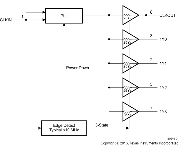
The CDCVF2505 is a high-performance, low-skew, low-jitter, phase-lock loop (PLL) clock
driver. This device uses a PLL to precisely align the output clocks (1Y[0-3] and CLKOUT) to the
input clock signal (CLKIN) in both frequency and phase. The CDCVF2505 operates at 3.3 V and also
provides integrated series-damping resistors that make it ideal for driving point-to-point
loads.One bank of five outputs provides low-skew, low-jitter copies of CLKIN. Output duty
cycles are adjusted to 50 percent, independent of duty cycle at CLKIN. The device automatically
goes into power-down mode when no input signal is applied to CLKIN. The loop filter for the PLLs is included on-chip. This minimizes the component count,
space, and cost.The CDCVF2505 is characterized for operation from –40°C to 85°C.Because it is based on the PLL circuitry, the CDCVF2505 requires a stabilization time to
achieve phase lock of the feedback signal to the reference signal. This stabilization is required
following power up and application of a fixed-frequency, fixed-phase signal at CLKIN, and following
any changes to the PLL reference.
CDCVF2505PWRG4 电路图