CDCP1803RGER 供应商
-
CDCP1803RGER
品牌:TI 封装/批号:原厂原装/22+ -
CDCP1803RGER
品牌:TI(德州仪器) 封装/批号:VQFN-24(4x4)/2022+ -
CDCP1803RGER
品牌:TI 封装/批号:标准封装/23+ -
CDCP1803RGER
品牌:TI 封装/批号:TSSOP/23+
CDCP1803RGER 属性参数
- 标准包装:3,000
- 类别:集成电路 (IC)
- 家庭:时钟/计时 - 时钟缓冲器,驱动器
- 系列:-
- 类型:扇出缓冲器(分配),除法器,多路复用器
- 电路数:1
- 比率 - 输入:输出:1:3
- 差分 - 输入:输出:是/是
- 输入:CML,HSTL,LVCMOS,LVDS,LVTTL,SSTL-2,VML
- 输出:LVPECL
- 频率 - 最大:800MHz
- 电源电压:3 V ~ 3.6 V
- 工作温度:-40°C ~ 85°C
- 安装类型:表面贴装
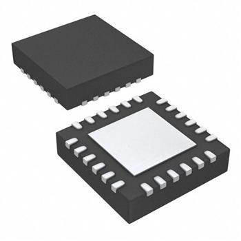
- 封装/外壳:24-VFQFN 裸露焊盘
- 供应商设备封装:24-VQFN 裸露焊盘(4x4)
- 包装:带卷 (TR)
产品特性
- Distributes One Differential Clock Input to Three LVPECL Differential Clock Outputs
- Programmable Output Divider for Two LVPECL Outputs
- Low-Output Skew 15 ps (Typical)
- VCC Range 3 V–3.6 V
- Signaling Rate Up to 800-MHz LVPECL
- Differential Input Stage for Wide Common-Mode Range
- Provides VBB Bias Voltage Output for Single-Ended Input Signals
- Receiver Input Threshold ±75 mV
- 24-Terminal QFN Package (4 mm × 4 mm)
- Accepts Any Differential Signaling: LVDS, HSTL, CML, VML, SSTL-2, and Single-Ended: LVTTL/LVCMOS
产品概述
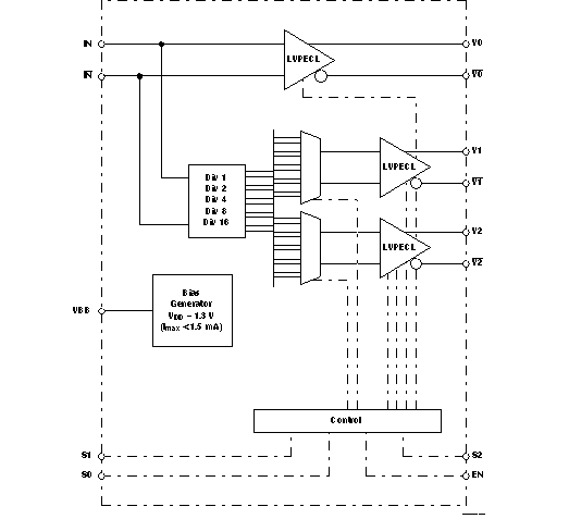
The CDCP1803 clock driver distributes one pair of differential clock inputs to three
pairs of LVPECL differential clock outputs Y[2:0] and Y[2:0] with minimum
skew for clock distribution. The CDCP1803 is specifically designed for driving 50-Ω transmission
lines.The CDCP1803 has three control terminals, S0, S1, and S2, to select different output mode
settings; see
for details. The CDCP1803 is characterized for operation from –40°C to 85°C. For use in
single-ended driver applications, the CDCP1803 also provides a VBB output terminal that can be
directly connected to the unused input as a common-mode voltage reference.
CDCP1803RGER 电路图