CDCM7005RGZR 供应商
-
CDCM7005RGZR
品牌:TI 封装/批号:原厂原装/22+ -
CDCM7005RGZR
品牌:TI 封装/批号:TSSOP/23+ -
CDCM7005RGZR
品牌:TI/德州仪器 封装/批号:VQFN48/21+ -
CDCM7005RGZR
品牌:TI/德州仪器 封装/批号:VQFN48/2022+ -
CDCM7005RGZRG4
品牌:TI 封装/批号:QFN48/23+
CDCM7005RGZR 属性参数
- 标准包装:2,500
- 类别:集成电路 (IC)
- 家庭:时钟/计时 - 时钟发生器,PLL,频率合成器
- 系列:-
- 类型:时钟同步器和抖动消除器
- PLL:带旁路
- 输入:LVCMOS,LVPECL
- 输出:LVCMOS,LVPECL
- 电路数:1
- 比率 - 输入:输出:3:10
- 差分 - 输入:输出:是/是
- 频率 - 最大:1.5GHz
- 除法器/乘法器:是/无
- 电源电压:3 V ~ 3.6 V
- 工作温度:-40°C ~ 85°C
- 安装类型:表面贴装
- 封装/外壳:48-VFQFN 裸露焊盘
- 供应商设备封装:48-VQFN 裸露焊盘(7x7)
- 包装:带卷 (TR)
- 配用:296-31328-ND - MODULE PATTERN GENERATOR BOARDTSW3070EVM-ND - TSW3070EVM296-31327-ND - KIT RF TRANSMIT CHAIN DEMO296-30827-ND - EVAL MODULE FOR CDCE72010CDCE421EVM-ND - CDCE421EVM296-20836-ND - EVALUATION MOD FOR CDCM7005-QFN296-20835-ND - EVALUATION MOD FOR CDCM7005-BGA296-20834-ND - EVALUATION MOD FOR CDC7005-QFN
产品特性
- High Performance LVPECL and LVCMOS PLL Clock Synchronizer
- Two Reference Clock Inputs (Primary and Secondary Clock) for Redundancy Support With Manual or Automatic Selection
- Accepts LVCMOS Input Frequencies up to 200 MHz
- VCXO_IN Clock is Synchronized to One of the Two Reference Clocks
- VCXO_IN Frequencies Up to 2.2 GHz (LVPECL)
- Outputs Can Be a Combination of LVPECL and LVCMOS (Up to Five Differential LVPECL Outputs or up to 10 LVCMOS Outputs)
- Output Frequency is Selectable by ×1, /2, /3, /4, /6, /8, /16 on Each Output Individually
- Efficient Jitter Cleaning From Low PLL Loop Bandwidth
- Low Phase Noise PLL Core
- Programmable Phase Offset (PRI_REF and SEC_REF to Outputs)
- Wide Charge Pump Current Range From 200 µA to 3 mA
- Dedicated Charge Pump Supply (VCC_CP) for Wide Tuning Voltage Range VCOs
- Presets Charge Pump to VCC_CP/2 for Fast Center-Frequency Setting of VC(X)O
- Analog and Digital PLL Lock Indication
- Provides VBB Bias Voltage Output for Single-Ended Input Signals (VCXO_IN)
- Frequency Hold-Over Mode Improves Fail-Safe Operation
- Power-up Control Forces LVPECL Outputs to 3-State at VCC < 1.5 V
- SPI Controllable Device Setting
- 3.3-V Power Supply
- Packaged in 64-Pin BGA (0.8 mm Pitch – ZVA) or 48-Pin QFN (RGZ)
- Industrial Temperature Range –40°C to 85°C
产品概述
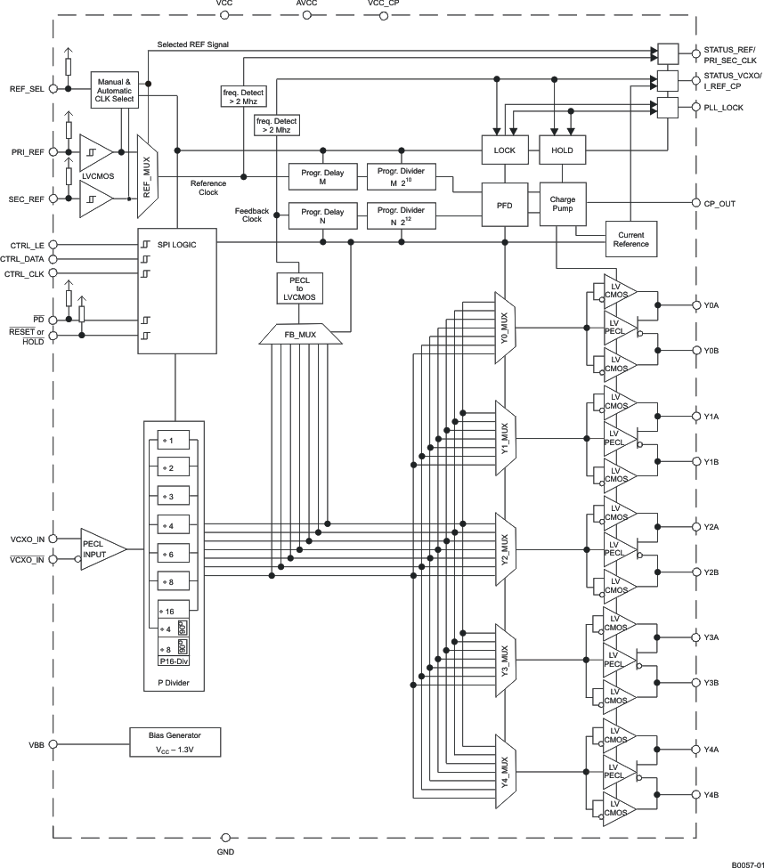
The CDCM7005 is a high-performance, low phase noise and low skew clock synchronizer that
synchronizes a VCXO (voltage controlled crystal oscillator) or VCO (voltage controlled oscillator)
frequency to one of the two reference clocks. The programmable pre-divider M and the
feedback-dividers N and P give a high flexibility to the frequency ratio of the reference clock to
VC(X)OVC(X)O_IN clock operates up to 2.2 GHz. Through the selection of external VC(X)O and loop
filter components, the PLL loop bandwidth and damping factor can be adjust to meet different system
requirements.The CDCM7005 can lock to one of two reference clock inputs (PRI_REF and SEC_REF),
supports frequency hold-over mode and fast-frequency-locking for fail-safe and increased system
redundancy. The outputs of the CDCM7005 are user definable and can be any combination of up to five
LVPECL outputs or up to 10 LVCMOS outputs. The built in synchronization latches ensure that all
outputs are synchronized for low output skew.All device settings, like outputs signaling, divider value, and input selection are
programmable by SPI (3-wire serial peripheral interface). SPI allows individually control of the
device settings.The device operates in 3.3-V environment and is characterized for operation from –40°C to
85°C.
CDCM7005RGZR 数据手册
CDCM7005RGZR 电路图