CDCLVP2106RHAR 供应商
-
CDCLVP2106RHAR
品牌:TI 封装/批号:原厂原装/22+ -
CDCLVP2106RHAR
品牌:TI(德州仪器) 封装/批号:VQFN-40(6x6)/2022+
CDCLVP2106RHAR 属性参数
- 标准包装:2,500
- 类别:集成电路 (IC)
- 家庭:时钟/计时 - 时钟缓冲器,驱动器
- 系列:-
- 类型:扇出缓冲器(分配)
- 电路数:2
- 比率 - 输入:输出:1:12
- 差分 - 输入:输出:是/是
- 输入:LVCMOS,LVDS,LVPECL,LVTTL
- 输出:LVPECL
- 频率 - 最大:2GHz
- 电源电压:2.375 V ~ 3.6 V
- 工作温度:-40°C ~ 85°C
- 安装类型:表面贴装
- 封装/外壳:40-VFQFN 裸露焊盘
- 供应商设备封装:40-VQFN-EP(6x6)
- 包装:带卷 (TR)
产品特性
- Dual 1:6 Differential Buffer
- Two Clock Inputs
- Universal Inputs Can Accept LVPECL, LVDS, LVCMOS/LVTTL
- 12 LVPECL Outputs
- Maximum Clock Frequency: 2 GHz
- Maximum Core Current Consumption: 92 mA
- Very Low Additive Jitter: <100 fs, RMS in 10-kHz to 20-MHz Offset Range
- 2.375-V to 3.6-V Device Power Supply
- Maximum Propagation Delay: 550 ps
- Maximum Within Bank Output Skew: 20 ps
- LVPECL Reference Voltage, VAC_REF, Available for Capacitive-Coupled Inputs
- Industrial Temperature Range: –40°C to +85°C
- Supports 105°C PCB Temperature (Measured with a Thermal Pad)
- Available in 6-mm × 6-mm, 40-Pin VQFN (RHA) Package
- ESD Protection Exceeds 2000 V (HBM)
产品概述
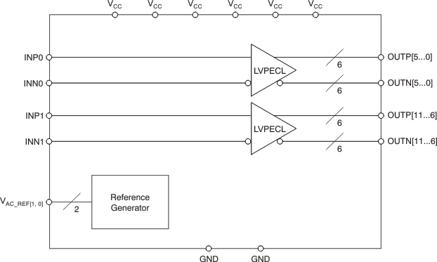
The CDCLVP2106 is a highly versatile, low additive jitter buffer that can generate 12
copies of LVPECL clock outputs from two LVPECL, LVDS, or LVCMOS inputs for a variety of
communication applications. It has a maximum clock frequency up to 2 GHz. Each buffer block
consists of one input that feeds two LVPECL outputs. The overall additive jitter performance is
less than 0.1 ps, RMS from 10 kHz to 20 MHz, and overall output skew is as low as 20 ps, making the
device a perfect choice for use in demanding applications.The CDCLVP2106 clock buffer distributes two clock inputs (IN0, IN1) to 12 pairs of
differential LVPECL clock outputs (OUT0, OUT11) with minimum skew for clock distribution. Each
buffer block consists of one input that feeds two LVPECL clock outputs. The inputs can be LVPECL,
LVDS, or LVCMOS/LVTTL.The CDCLVP2106 is specifically designed for driving 50-Ω transmission lines. When driving
the inputs in single-ended mode, the LVPECL bias voltage (VAC_REF) should be
applied to the unused negative input pin. However, for high-speed performance up to 2 GHz,
differential mode is strongly recommended.The CDCLVP2106 is characterized for operation from –40°C to +85°C and is available in a
6-mm × 6-mm, VQFN-40 package.
CDCLVP2106RHAR 电路图