CDCLVP1208RHDT 供应商
-
CDCLVP1208RHDT
品牌:TI 封装/批号:原厂原装/22+ -
CDCLVP1208RHDT
品牌:TI(德州仪器) 封装/批号:VQFN-28/2022+ -
CDCLVP1208RHDT
品牌:TI 封装/批号:原厂原封装/新批号 -
CDCLVP1208RHDT
品牌:TI 封装/批号:TSSOP/23+
CDCLVP1208RHDT 属性参数
- 标准包装:1
- 类别:集成电路 (IC)
- 家庭:时钟/计时 - 时钟缓冲器,驱动器
- 系列:-
- 类型:扇出缓冲器(分配),多路复用器
- 电路数:1
- 比率 - 输入:输出:2:8
- 差分 - 输入:输出:是/是
- 输入:LVCMOS,LVDS,LVPECL,LVTTL
- 输出:LVPECL
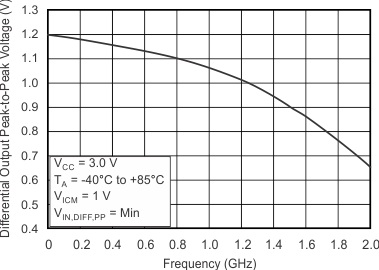
- 频率 - 最大:2GHz
- 电源电压:2.375 V ~ 3.6 V
- 工作温度:-40°C ~ 85°C
- 安装类型:表面贴装
- 封装/外壳:28-VFQFN 裸露焊盘
- 供应商设备封装:28-VQFN-EP(5x5)
- 包装:®
- 其它名称:296-25302-6
产品特性
- 2:8 Differential Buffer
- Selectable Clock Inputs Through Control terminal
- Universal Inputs Accept LVPECL, LVDS, and LVCMOS/LVTTL
- Eight LVPECL Outputs
- Maximum Clock Frequency: 2 GHz
- Maximum Core Current Consumption: 73 mA
- Very Low Additive Jitter: <100 fs,rms in 10 kHz to 20 MHz Offset Range: 57 fs, rms (typical) at 122.88 MHz 48 fs, rms (typical) at 156.25 MHz 30 fs, rms (typical) at 312.5 MHz
- 57 fs, rms (typical) at 122.88 MHz
- 48 fs, rms (typical) at 156.25 MHz
- 30 fs, rms (typical) at 312.5 MHz
- 2.375-V to 3.6-V Device Power Supply
- Maximum Propagation Delay: 450 ps
- Maximum Output Skew: 20 ps
- LVPECL Reference Voltage, VAC_REF, Available for Capacitive-Coupled Inputs
- Industrial Temperature Range: –40°C to 85°C
- Supports 105°C PCB Temperature (Measured with a Thermal Pad)
- ESD Protection Exceeds 2 kV (HBM)
- Available in 5-mm × 5-mm QFN-28 (RHD) Package
产品概述
The CDCLVP1208 is a highly versatile, low additive jitter buffer that can generate eight
copies of LVPECL clock outputs from one of two selectable LVPECL, LVDS, or LVCMOS inputs for a
variety of communication applications. It has a maximum clock frequency up to 2 GHz. The CDCLVP1208
features an on-chip multiplexer (MUX) for selecting one of two inputs that can be easily configured
solely through a control terminal. The overall additive jitter performance is less than 0.1 ps, RMS
from 10 kHz to 20 MHz, and overall output skew is as low as 20 ps, making the device a perfect
choice for use in demanding applications.The CDCLVP1208 clock buffer distributes one of two selectable clock inputs (IN0, IN1) to
eight pairs of differential LVPECL clock outputs (OUT0, OUT7) with minimum skew for clock
distribution. The CDCLVP1208 can accept two clock sources into an input multiplexer. The inputs can
be LVPECL, LVDS, or LVCMOS/LVTTL.The CDCLVP1208 is specifically designed for driving 50-Ω transmission lines. When driving
the inputs in single-ended mode, the LVPECL bias voltage (VAC_REF) should be
applied to the unused negative input terminal. However, for high-speed performance up to 2 GHz,
differential mode is strongly recommended. The CDCLVP1208 is packaged in a small 28-pin,
5-mm × 5-mm QFN package and is characterized for operation from –40°C to 85°C.
CDCLVP1208RHDT 电路图