CDCLVP110VF 供应商
-
CDCLVP110VF
品牌:TI 封装/批号:原厂原装/22+ -
CDCLVP110VF
品牌:TI/德州仪器 封装/批号:LQFP32/21+ -
CDCLVP110VF
品牌:TI 封装/批号:TQFP/23+ -
CDCLVP110VF
品牌:TI 封装/批号:QFP/21+ -
CDCLVP110VF
品牌: 封装/批号:/22+ -
CDCLVP110VF
品牌:TI 封装/批号:TSSOP/23+ -
CDCLVP110VFR
品牌:TI(德州仪器) 封装/批号:LQFP-32/2022+
CDCLVP110VF 属性参数
- 标准包装:250
- 类别:集成电路 (IC)
- 家庭:时钟/计时 - 时钟缓冲器,驱动器
- 系列:-
- 类型:扇出缓冲器(分配),多路复用器
- 电路数:1
- 比率 - 输入:输出:2:10
- 差分 - 输入:输出:是/是
- 输入:HSTL,LVPECL
- 输出:LVPECL
- 频率 - 最大:3.5GHz
- 电源电压:2.375 V ~ 3.8 V
- 工作温度:-40°C ~ 85°C
- 安装类型:表面贴装
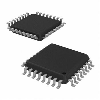
- 封装/外壳:32-LQFP
- 供应商设备封装:32-LQFP(7x7)
- 包装:托盘
- 其它名称:296-15357
产品特性
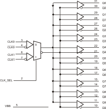
- Distributes One Differential Clock Input Pair LVPECL/HSTL to 10 Differential LVPECL Clock Outputs
- Fully Compatible With LVECL/LVPECL/HSTL
- Single Supply Voltage Required, ±3.3-V or ±2.5-V Supply
- Selectable Clock Input Through CLK_SEL
- Low-Output Skew (Typ 15 ps) for Clock-Distribution Applications
- VBB Reference Voltage Output for Single-Ended Clocking
- Available in a 32-Pin LQFP Package
- Frequency Range From DC to 3.5 GHz
- Pin-to-Pin Compatible With MC100 Series EP111, ES6111, LVEP111, PTN1111
产品概述
The CDCLVP110 clock driver distributes one differential clock pair of either LVPECL or HSTL (selectable) input, (CLK0, CLK1) to ten pairs of differential LVPECL clock (Q0, Q9) outputs with minimum skew for clock distribution. The CDCLVP110 can accept two clock sources into an input multiplexer. The CLK0 input accepts either LVECL/LVPECL input signals, while CLK1 accepts an HSTL input signal when operated under LVPECL conditions. The CDCLVP110 is specifically designed for driving 50-Ω transmission lines.The VBB reference voltage output is used if single-ended input operation is required. In this case the VBB pin should be connected to CLK0 and bypassed to GND via a 10-nF capacitor.However, for high-speed performance up to 3.5 GHz, the differential mode is strongly recommended.The CDCLVP110 is characterized for operation from –40°C to 85°C.
CDCLVP110VF 数据手册
CDCLVP110VF 电路图