CDCLVP1102RGTR 供应商
-
CDCLVP1102RGTR
品牌:TI 封装/批号:原厂原装/22+ -
CDCLVP1102RGTR
品牌:TI 封装/批号:/23+ -
CDCLVP1102RGTR
品牌:TI/德州仪器 封装/批号:QFN16/21+ -
CDCLVP1102RGTR
品牌:TI(德州仪器) 封装/批号:QFN-16(3x3)/2022+ -
CDCLVP1102RGTR
品牌: 封装/批号:TSSOP/23+
CDCLVP1102RGTR 属性参数
- 标准包装:1
- 类别:集成电路 (IC)
- 家庭:时钟/计时 - 时钟缓冲器,驱动器
- 系列:-
- 类型:扇出缓冲器(分配)
- 电路数:1
- 比率 - 输入:输出:1:2
- 差分 - 输入:输出:是/是
- 输入:LVCMOS,LVDS,LVPECL,LVTTL
- 输出:LVPECL
- 频率 - 最大:2GHz
- 电源电压:2.375 V ~ 3.6 V
- 工作温度:-40°C ~ 85°C
- 安装类型:表面贴装
- 封装/外壳:16-VFQFN 裸露焊盘
- 供应商设备封装:16-QFN-EP(3x3)
- 包装:®
- 其它名称:296-31621-6
产品特性
- 1:2 Differential Buffer
- Single Clock Input
- Universal Inputs Can Accept LVPECL, LVDS, LVCMOS/LVTTL
- Two LVPECL Outputs
- Maximum Clock Frequency: 2 GHz
- Maximum Core Current Consumption: 33 mA
- Very Low Additive Jitter: <100 fs, RMS in 10-kHz to 20-MHz Offset Range
- 2.375-V to 3.6-V Device Power Supply
- Maximum Propagation Delay: 450 ps
- Maximum Output Skew: 10 ps
- LVPECL Reference Voltage, VAC_REF, Available for Capacitive-Coupled Inputs
- Industrial Temperature Range: –40°C to 85°C
- Supports 105°C PCB Temperature (Measured at Thermal Pad)
- Available in 3-mm × 3-mm QFN-16 (RGT) Package
- ESD Protection Exceeds 2 kV (HBM)
产品概述
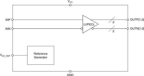
The CDCLVP1102 is a highly versatile, low additive jitter buffer that can generate two
copies of LVPECL clock outputs from one LVPECL, LVDS, or LVCMOS input for a variety of
communication applications. It has a maximum clock frequency up to 2 GHz. The overall additive
jitter performance is less than 0.1 ps, RMS from 10 kHz to 20 MHz, and overall output skew is as
low as 10 ps, making the device a perfect choice for use in demanding applications.The CDCLVP1102 clock buffer distributes a single clock input (IN) to two pairs of
differential LVPECL clock outputs (OUT0, OUT1) with minimum skew for clock distribution. The inputs
can be LVPECL, LVDS, or LVCMOS/LVTTL.The CDCLVP1102 is specifically designed for driving 50-Ω transmission lines. When driving
the inputs in single-ended mode, the LVPECL bias voltage (VAC_REF) should be
applied to the unused negative input pin. However, for high-speed performance up to 2 GHz,
differential mode is strongly recommended.The CDCLVP1102 is characterized for operation from –40°C to 85°C and is available in a
QFN-16, 3-mm × 3-mm package.
CDCLVP1102RGTR 电路图