CDCLVD1213RGTT 供应商
-
CDCLVD1213RGTT
品牌:TI 封装/批号:原厂原装/22+ -
CDCLVD1213RGTT
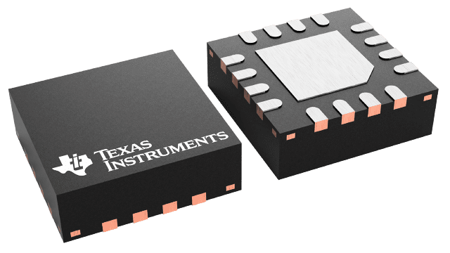
品牌:TI(德州仪器) 封装/批号:VQFN-16/2022+ -
CDCLVD1213RGTT
品牌:TI 封装/批号:/23+ -
CDCLVD1213RGTT
品牌:TI 封装/批号:TSSOP/23+
CDCLVD1213RGTT 属性参数
- 标准包装:1
- 类别:集成电路 (IC)
- 家庭:时钟/计时 - 时钟缓冲器,驱动器
- 系列:-
- 类型:扇出缓冲器(分配),除法器
- 电路数:1
- 比率 - 输入:输出:1:4
- 差分 - 输入:输出:是/是
- 输入:CML,LVDS,LVPECL
- 输出:LVDS
- 频率 - 最大:800MHz
- 电源电压:2.375 V ~ 2.625 V
- 工作温度:-40°C ~ 85°C
- 安装类型:表面贴装
- 封装/外壳:16-VFQFN 裸露焊盘
- 供应商设备封装:16-QFN-EP(3x3)
- 包装:®
- 其它名称:296-27761-6
产品特性
- 1:4 Differential Buffer
- Low Additive Jitter: < 300-fs RMS in 10-kHz to 20-MHz
- Low Output Skew of 20 ps (Maximum)
- Selectable Divider Ratio 1, /2, /4
- Universal Input Accepts LVDS, LVPECL, and CML
- 4 LVDS Outputs, ANSI EIA/TIA-644A Standard Compatible
- Clock Frequency: Up to 800 MHz
- Device Power Supply: 2.375 V to 2.625 V
- Industrial Temperature Range: –40°C to 85°C
- Packaged in 3 mm × 3 mm, 16-Pin VQFN (RGT)
- ESD Protection Exceeds 3-kV HBM, 1-kV CDM
- APPLICATIONS Telecommunications and Networking Medical Imaging Test and Measurement Equipment Wireless Communications General-Purpose Clocking
- Telecommunications and Networking
- Medical Imaging
- Test and Measurement Equipment
- Wireless Communications
- General-Purpose Clocking
产品概述
The CDCLVD1213 clock buffer distributes an input clock to 4 pairs of differential LVDS
clock outputs with low additive jitter for clock distribution. The input can either be LVDS,
LVPECL, or CML.The CDCLVD1213 contains a high performance divider for one output (QD) which can divide
the input clock signal by a factor of 1, 2, or 4.The CDCLVD1213 is specifically designed for driving 50-Ω transmission lines. The part
supports a fail-safe function. The device incorporates an input hysteresis which prevents random
oscillation of the outputs in the absence of an input signal. The device operates in 2.5-V supply environment and is characterized from –40°C to 85°C
(ambient temperature). The CDCLVD1213 is packaged in small, 16-pin, 3-mm × 3-mm VQFN
package.