CDCLVD1208RHDR 供应商
-
CDCLVD1208RHDR
品牌:TI 封装/批号:原厂原装/22+ -
CDCLVD1208RHDR
品牌:TI/德州仪器 封装/批号:QFN/21+ -
CDCLVD1208RHDR
品牌:TI(德州仪器) 封装/批号:VQFN-28/2022+ -
CDCLVD1208RHDR
品牌:TI 封装/批号:原厂原封装/新批号 -
CDCLVD1208RHDR
品牌:TI 封装/批号:/2021+ -
CDCLVD1208RHDR
品牌: 封装/批号:/23+
CDCLVD1208RHDR 属性参数
- 标准包装:3,000
- 类别:集成电路 (IC)
- 家庭:时钟/计时 - 时钟缓冲器,驱动器
- 系列:-
- 类型:扇出缓冲器(分配),多路复用器
- 电路数:1
- 比率 - 输入:输出:2:8
- 差分 - 输入:输出:是/是
- 输入:LVCMOS,LVDS,LVPECL
- 输出:LVDS
- 频率 - 最大:800MHz
- 电源电压:2.375 V ~ 2.625 V
- 工作温度:-40°C ~ 85°C
- 安装类型:表面贴装
- 封装/外壳:28-VFQFN 裸露焊盘
- 供应商设备封装:28-VQFN-EP(5x5)
- 包装:带卷 (TR)
产品特性
- 2:8 Differential Buffer
- Low Additive Jitter: < 300-fs RMS in 10-kHz to 20-MHz
- Low Output Skew of 45 ps (Maximum)
- Universal Inputs Accept LVDS, LVPECL, and LVCMOS
- Selectable Clock Inputs Through Control Pin
- 8 LVDS Outputs, ANSI EIA/TIA-644A Standard Compatible
- Clock Frequency: Up to 800 MHz
- Device Power Supply: 2.375 V to 2.625 V
- LVDS Reference Voltage, VAC_REF, Available for Capacitive Coupled Inputs
- Industrial Temperature Range: –40°C to 85°C
- Packaged in 5-mm × 5-mm, 28-Pin VQFN (RHD)
- ESD Protection Exceeds 3-kV HBM, 1-kV CDM
- APPLICATIONS Telecommunications and Networking Medical Imaging Test and Measurement Equipment Wireless Communications General-Purpose Clocking
- Telecommunications and Networking
- Medical Imaging
- Test and Measurement Equipment
- Wireless Communications
- General-Purpose Clocking
产品概述
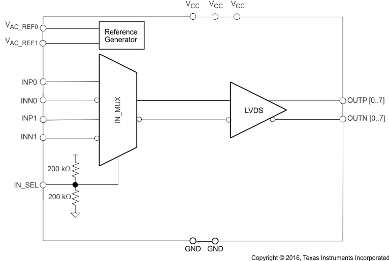
The CDCLVD1208 clock buffer distributes one of two selectable clock inputs (IN0 and IN1)
to 8 pairs of differential LVDS clock outputs (OUT0 through OUT7) with minimum skew for clock
distribution. The CDCLVD1208 can accept two clock sources into an input multiplexer. The inputs can
either be LVDS, LVPECL, or LVCMOS.The CDCLVD1208 is specifically designed for driving 50-Ω transmission lines. In case of
driving the inputs in single-ended mode, the appropriate bias voltage,
VAC_REF, must be applied to the unused negative input pin.The IN_SEL pin selects the input which is routed to the outputs. If this pin is left
open, it disables the outputs (static). The part supports a fail-safe function. The device
incorporates an input hysteresis which prevents random oscillation of the outputs in the absence of
an input signal.The device operates in 2.5-V supply environment and is characterized from –40°C to 85°C
(ambient temperature). The CDCLVD1208 is packaged in small, 28-pin, 5-mm × 5-mm VQFN
package.
CDCLVD1208RHDR 电路图