CDCLVD110ARHBR 供应商
-
CDCLVD110ARHBR
品牌:TI 封装/批号:原厂原装/22+ -
CDCLVD110ARHBR
品牌: 封装/批号:/23+ -
CDCLVD110ARHBR
品牌:TI/德州仪器 封装/批号:VQFN32/21+ -
CDCLVD110ARHBR
品牌:TI/德州仪器 封装/批号:VQFN32/2022+ -
CDCLVD110ARHBRG4
品牌:TI 封装/批号:QFN/23+
CDCLVD110ARHBR 属性参数
- 标准包装:3,000
- 类别:集成电路 (IC)
- 家庭:时钟/计时 - 时钟缓冲器,驱动器
- 系列:-
- 类型:扇出缓冲器(分配),多路复用器
- 电路数:1
- 比率 - 输入:输出:2:10
- 差分 - 输入:输出:是/是
- 输入:LVDS
- 输出:LVDS
- 频率 - 最大:1.1GHz
- 电源电压:2.375 V ~ 2.625 V
- 工作温度:-40°C ~ 85°C
- 安装类型:表面贴装
- 封装/外壳:32-VFQFN 裸露焊盘
- 供应商设备封装:32-QFN 裸露焊盘(5x5)
- 包装:带卷 (TR)
产品特性
- Low-Output Skew <30 ps (Typical) for Clock-Distribution Applications
- Distributes One Differential Clock Input to 10 LVDS Differential Clock Outputs
- VCC Range: 2.5 V ±5%
- Typical Signaling Rate Capability of Up to 1.1 GHz
- Configurable Register (SI/CK) Individually Enables Disables Outputs, Selectable CLK0, CLK0 or CLK1, CLK1 Inputs
- Full Rail-to-Rail Common-Mode Input Range
- Receiver Input Threshold: ±100 mV
- Available in 32-Pin LQFP and VQFN Package
- Fail-Safe I/O-Pins for VDD = 0 V (Power Down)
产品概述
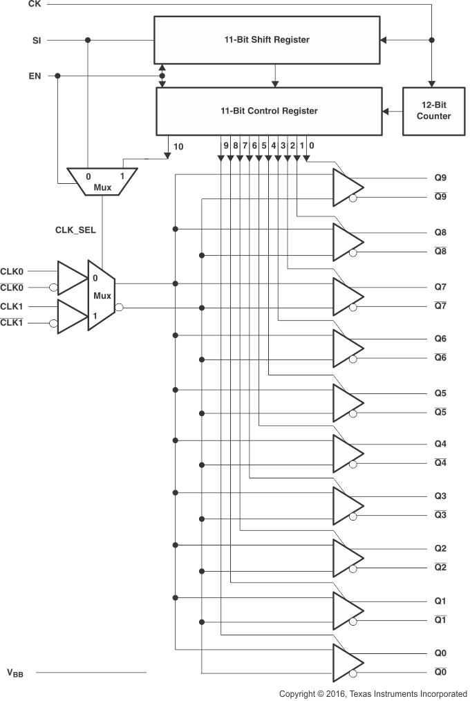
The CDCLVD110A clock driver distributes one pair of differential LVDS clock inputs
(either CLK0 or CLK1) to 10 pairs of differential clock outputs (Q0 to Q9) with minimum skew for
clock distribution. The CDCLVD110A is specifically designed to drive 50-Ω transmission
lines.When the control enable is high (EN = 1), the 10 differential outputs are programmable in
that each output can be individually enabled or disabled
(3-stated) according to the first 10 bits loaded into the shift register. Once the shift
register is loaded, the last bit selects either CLK0 or CLK1 as the clock input. However, when EN =
0, the outputs are not programmable and all outputs are enabled. The CDCLVD110A has an improved start-up circuit that minimizes enabling time in AC- and
DC-coupled systems.The CDCLVD110A is characterized for operation from –40°C to 85°C.
CDCLVD110ARHBR 电路图