CDCL1810RGZR 供应商
-
CDCL1810RGZR
品牌:TI 封装/批号:原厂原装/22+ -
CDCL1810RGZR
品牌:TI(德州仪器) 封装/批号:VQFN-48(7x7)/2022+ -
CDCL1810RGZR
品牌:TI 封装/批号:TSSOP/23+
CDCL1810RGZR 属性参数
- 标准包装:2,500
- 类别:集成电路 (IC)
- 家庭:时钟/计时 - 时钟缓冲器,驱动器
- 系列:-
- 类型:扇出缓冲器(分配),除法器
- 电路数:1
- 比率 - 输入:输出:1:10
- 差分 - 输入:输出:是/是
- 输入:LVDS
- 输出:CML
- 频率 - 最大:650MHz
- 电源电压:1.7 V ~ 1.9 V
- 工作温度:-40°C ~ 85°C
- 安装类型:表面贴装
- 封装/外壳:48-VFQFN 裸露焊盘
- 供应商设备封装:48-VQFN 裸露焊盘(7x7)
- 包装:带卷 (TR)
产品特性
- Single 1.8-V Supply
- High-Performance Clock Distributor with 10 Outputs
- Low Input-to-Output Additive Jitter: as Low as 10fs RMS
- Output Group Phase Adjustment
- Low-Voltage Differential Signaling (LVDS) Input, 100-Ω Differential On-Chip Termination, up to 650 MHz Frequency
- Differential Current Mode Logic (CML) Outputs, 50-Ω Single-Ended On-Chip Termination, up to 650 MHz Frequency
- Two Groups of Five Outputs Each with Independent Frequency Division Ratios
- Output Frequency Derived with Divide Ratios of 1, 2, 4, 5, 8, 10, 16, 20, 32, 40, and 80
- Meets ANSI TIA/EIA-644-A-2001 LVDS Standard Requirements
- Power Consumption: 410 mW Typical
- Output Enable Control for Each Output and Automatic Output Synchronization
- SDA/SCL Device Management Interface
- 48-pin VQFN (RGZ) Package
- Industrial Temperature Range: –40°C to +85°C
产品概述
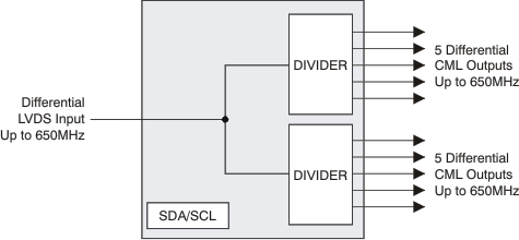
The CDCL1810 is a high-performance clock distributor. The programmable dividers, P0 and
P1, give a high flexibility to the ratio of the output frequency to the input frequency:
FOUT = FIN/P, where: P (P0,P1) = 1, 2, 4, 5, 8, 10,
16, 20, 32, 40, 80. The CDCL1810 supports one differential LVDS clock input and a total of 10 differential
CML outputs. The CML outputs are compatible with LVDS receivers if they are ac-coupled.With careful observation of the input voltage swing and common-mode voltage limits, the
CDCL1810 can support a single-ended clock input as outlined in Pin Configuration and Functions.All device settings are programmable through the SDA/SCL, serial two-wire interface.
The serial interface is 1.8V tolerant only.The phase of one output group relative to the other can be adjusted through the SDA/SCL
interface. For post-divide ratios (P0, P1) that are multiples of 5, the total number of phase
adjustment steps (η) equals the divide-ratio divided by 5. For
post-divide ratios (P0, P1) that are not multiples of 5, the total number of steps (η) is the same as the post-divide ratio. The phase adjustment step (ΔΦ) in
time units is given as: ΔΦ = 1/(n × FOUT), where FOUT
is the respective output frequency.The device operates in a 1.8-V supply environment and is characterized for operation from
–40°C to +85°C. The CDCL1810 is available in a 48-pin VQFN (RGZ) package.
CDCL1810RGZR 电路图