CDCE925PWG4 供应商
-
CDCE925PWG4
品牌:TI 封装/批号:原厂原装/22+ -
CDCE925PWG4
品牌:TI(德州仪器) 封装/批号:TSSOP-16/2022+
CDCE925PWG4 属性参数
- 视频文件:ClockPro Programming Software Demo
- 标准包装:90
- 类别:集成电路 (IC)
- 家庭:时钟/计时 - 时钟发生器,PLL,频率合成器
- 系列:-
- 类型:PLL 时钟发生器
- PLL:带旁路
- 输入:LVCMOS,晶体
- 输出:LVCMOS
- 电路数:1
- 比率 - 输入:输出:1:5
- 差分 - 输入:输出:无/无
- 频率 - 最大:230MHz
- 除法器/乘法器:是/无
- 电源电压:1.7 V ~ 1.9 V
- 工作温度:-40°C ~ 85°C
- 安装类型:表面贴装
- 封装/外壳:16-TSSOP(0.173",4.40mm 宽)
- 供应商设备封装:16-TSSOP
- 包装:管件
- 配用:296-30836-ND - EEPROM PROG MODULE FOR CDCEL9XX296-30831-ND - EVAL MOD PERFORMANCE FOR CDCE914
- 其它名称:296-27962-5CDCE925PWG4-ND
产品特性
- Member of Programmable Clock Generator Family CDCEx913: 1-PLL, 3 Outputs CDCEx925: 2-PLL, 5 Outputs CDCEx925: 3-PLL, 7 Outputs CDCEx949: 4-PLL, 9 Outputs
- CDCEx913: 1-PLL, 3 Outputs
- CDCEx925: 2-PLL, 5 Outputs
- CDCEx925: 3-PLL, 7 Outputs
- CDCEx949: 4-PLL, 9 Outputs
- In-System Programmability and EEPROM Serial Programmable Volatile Register Nonvolatile EEPROM to Store Customer Settings
- Serial Programmable Volatile Register
- Nonvolatile EEPROM to Store Customer Settings
- Flexible Input Clocking Concept External Crystal: 8 MHz to 32 MHz On-Chip VCXO: Pull Range ±150 ppm Single-Ended LVCMOS Up to 160 MHz
- External Crystal: 8 MHz to 32 MHz
- On-Chip VCXO: Pull Range ±150 ppm
- Single-Ended LVCMOS Up to 160 MHz
- Free Selectable Output Frequency Up to 230 MHz
- Low-Noise PLL Core PLL Loop Filter Components Integrated Low Period Jitter (Typical 60 ps)
- PLL Loop Filter Components Integrated
- Low Period Jitter (Typical 60 ps)
- Separate Output Supply Pins CDCE925: 3.3 V and 2.5 V CDCEL925: 1.8 V
- CDCE925: 3.3 V and 2.5 V
- CDCEL925: 1.8 V
- Flexible Clock Driver Three User-Definable Control Inputs [S0/S1/S2], for Example, SSC Selection, Frequency Switching, Output Enable, or Power Down Generates Highly Accurate Clocks for Video, Audio, USB, IEEE1394, RFID, Bluetooth®, WLAN, Ethernet™, and GPS Generates Common Clock Frequencies Used With TI-DaVinci™, OMAP™, DSPs Programmable SSC Modulation Enables 0-PPM Clock Generation
- Three User-Definable Control Inputs [S0/S1/S2], for Example, SSC Selection, Frequency Switching, Output Enable, or Power Down
- Generates Highly Accurate Clocks for Video, Audio, USB, IEEE1394, RFID, Bluetooth®, WLAN, Ethernet™, and GPS
- Generates Common Clock Frequencies Used With TI-DaVinci™, OMAP™, DSPs
- Programmable SSC Modulation
- Enables 0-PPM Clock Generation
- 1.8-V Device Power Supply
- Wide Temperature Range: –40°C to 85°C
- Packaged in TSSOP
- Development and Programming Kit for Easy PLL Design and Programming (TI Pro-Clock™)
- APPLICATIONS D-TVs, STBs, IP-STBs, DVD Players, DVD Recorders, and Printers
- D-TVs, STBs, IP-STBs, DVD Players, DVD Recorders, and Printers
产品概述
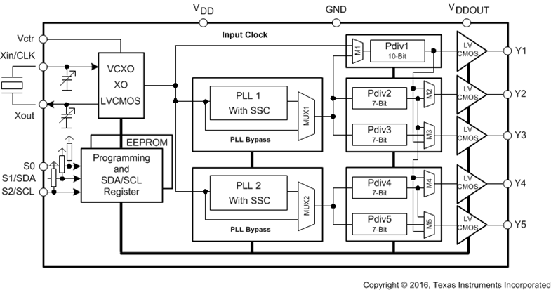
The CDCE925 and CDCEL925 are modular PLL-based low-cost, high-performance, programmable
clock synthesizers, multipliers, and dividers. They generate up to five output clocks from a single
input frequency. Each output can be programmed in-system for any clock frequency up to 230 MHz,
using up to two independent configurable PLLs.The CDCEx925 has a separate output supply pin, VDDOUT, which is
1.8 V for CDCEL925 and 2.5 V to 3.3 V for CDCE925.The input accepts an external crystal or LVCMOS clock signal. In case of a crystal input,
an on-chip load capacitor is adequate for most applications. The value of the load capacitor is
programmable from 0 to 20 pF. Additionally, an on-chip VCXO is selectable which allows
synchronization of the output frequency to an external control signal, that is, PWM signal.The deep M/N divider ratio allows the generation of zero-ppm audio/video, networking
(WLAN, Bluetooth, Ethernet, GPS), or interface (USB, IEEE1394, memory stick) clocks from a 27-MHz
reference input frequency, for example.All PLLs support SSC (spread-spectrum clocking). SSC can be center-spread or down-spread
clocking, which is a common technique to reduce electromagnetic interference (EMI). Based on the PLL frequency and the divider settings, the internal loop filter components
are automatically adjusted to achieve high stability and optimized jitter transfer characteristic
of each PLL.The device supports nonvolatile EEPROM programming for easy customization of the device
in the application. It is preset to a factory default configuration and can be reprogrammed to a
different application configuration before it goes onto the PCB or reprogrammed by in-system
programming. All device settings are programmable through the SDA/SCL bus, a 2-wire serial
interface.Three, free programmable control inputs, S0, S1, and S2, can be used to select different
frequencies, or change the SSC setting for lowering EMI, or other control features like outputs
disable to low, outputs in high-impedance state, power down, PLL bypass, and so forth.The CDCx925 operates in a 1.8-V environment and in a temperature range of –40°C to
85°C.
CDCE925PWG4 数据手册
CDCE925PWG4 电路图