CDC339DW 供应商
CDC339DW 属性参数
- 标准包装:25
- 类别:集成电路 (IC)
- 家庭:时钟/计时 - 时钟缓冲器,驱动器
- 系列:-
- 类型:扇出缓冲器(分配)
- 电路数:1
- 比率 - 输入:输出:1:8
- 差分 - 输入:输出:无/无
- 输入:TTL
- 输出:TTL
- 频率 - 最大:80MHz
- 电源电压:4.75 V ~ 5.25 V
- 工作温度:-40°C ~ 85°C
- 安装类型:表面贴装
- 封装/外壳:20-SOIC(0.295",7.50mm 宽)
- 供应商设备封装:20-SOIC
- 包装:管件
- 其它名称:296-6699-5
产品特性
- Low Output Skew, Low Pulse Skew for Clock-Distribution and Clock-Generation Applications
- TTL-Compatible Inputs and Outputs
- Distributes One Clock Input to Eight Outputs Four Same-Frequency Outputs Four Half-Frequency Outputs
- Four Same-Frequency Outputs
- Four Half-Frequency Outputs
- Distributed VCC and Ground Pins Reduce Switching Noise
- High-Drive Outputs (−48-mA IOH, 48-mA IOL)
- State-of-the-Art EPIC-ΙΙB™ BiCMOS Design Significantly Reduces Power Dissipation
- Package Options Include Plastic Small-Outline (DW) and Shrink Small-Outline (DB) Packages
产品概述
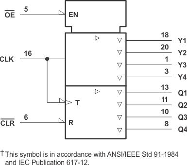
The CDC339 is a high-performance,
low-skew clock driver. It is specifically designed for applications requiring
synchronized output signals at both the primary clock frequency and one-half the
primary clock frequency. The four Y outputs switch in phase and at the same
frequency as the clock (CLK) input. The four Q outputs switch at one-half the
frequency of CLK. When the output-enable
(OE) input is low and the clear (CLR)
input is high, the Y outputs follow CLK and the Q outputs toggle on low-to-high
transitions of CLK. Taking CLR low asynchronously resets the Q
outputs to the low level. When OE is high, the outputs are in
the high-impedance state. The CDC339 is characterized for
operation from −40°C to 85°C.
CDC339DW 电路图