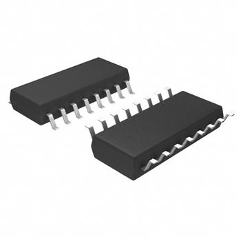
CD4502BNSR 供应商
-
CD4502BNSR
品牌:TI 封装/批号:原厂原装/22+ -
CD4502BNSR
品牌:TI(德州仪器) 封装/批号:SO-16/2022+
CD4502BNSR 属性参数
- 标准包装:1
- 类别:集成电路 (IC)
- 家庭:逻辑 - 栅极和逆变器
- 系列:4000B
- 逻辑类型:逆变器,缓冲器
- 电路数:6
- 输入数:1
- 特点:三态
- 电源电压:3 V ~ 18 V
- 电流 - 静态(最大值):4µA
- 输出电流高,低:3.4mA,20.4mA
- 逻辑电平 - 低:1.5 V ~ 4 V
- 逻辑电平 - 高:3.5 V ~ 11 V
- 额定电压和最大 CL 时的最大传播延迟:130ns @ 15V,50pF
- 工作温度:-55°C ~ 125°C
- 安装类型:表面贴装
- 供应商设备封装:16-SO
- 封装/外壳:16-SOIC(0.209",5.30mm 宽)
- 包装:®
- 其它名称:296-14148-6
产品特性
- 2 TTL-load output drive capability
- 3-state outputs
- Common output-disable control
- Inhibit control
- 100% tested for quiescent current at 20 V
- 5-V, 10-V, and 15-V parametric ratings
- Maximum input current of 1 µA at 18 V over full package-temperature range; 100 nA at 18 V and 25°C
- Meets all requirements of JEDEC Tentative Standard No. 13B, "Standard Specifications for Description of 'B' Series CMOS Devices"
- Noise Margin (full package-temperature range) = 1 V at VDD = 5 V 2 V at VDD = 10 V 2.5 V at VDD = 15 V
- Applications: 3-state hex inverter for interfacing IC's with data buses COS/MOS to TTL hex buffer
- 3-state hex inverter for interfacing IC's with data buses
- COS/MOS to TTL hex buffer
产品概述
CD4502B consists of six inverter/buffers with 3-state outputs. A logic "1" on the OUTPUT DISABLE input produces a high-impedance state in all six outputs. This feature permits common busing of the outputs, thus simplifying system design. A Logic "1" on the INHIBIT input switches all six outputs to logic "0" if the OUTPUT DISABLE input is a logic "0". This device is capable of driving two standard TTL loads, which is equivalent to six times the JEDEC "B"-series IOL standard.The CD4502B types are supplied in 16-lead hermetic dual-in-line ceramic packages (F3A suffix), 16-lead dual-in-line plastic packages (E suffix), 16-lead small-outline packages (NSR suffix), and 16-lead thin shrink small-outline packages (PW and PWR suffixes).
