CD4013BM 供应商
-
CD4013BM
品牌:TI 封装/批号:原厂原装/22+ -
CD4013BM
品牌:TI 封装/批号:/2021+ -
CD4013BM
品牌:TI 封装/批号:14SOIC/2019+ -
CD4013BM
品牌:TI 封装/批号:SOP14/22+授权代理 -
CD4013BM
品牌:TI(德州仪器) 封装/批号:SOIC-14/2022+ -
CD4013BM
品牌:TI 封装/批号:SO-14/7 -
CD4013BM
品牌:NXP 封装/批号:SOP14/新批号 -
CD4013BM96
品牌:TI 封装/批号:SOP-14/ -
CD4013BM96
品牌:TI 封装/批号:SOP-14/23+ -
CD4013BM96
品牌: 封装/批号:/连可连代销V
CD4013BM 属性参数
- 标准包装:50
- 类别:集成电路 (IC)
- 家庭:逻辑 - 触发器
- 系列:4000B
- 功能:设置(预设)和复位
- 类型:D 型
- 输出类型:差分
- 元件数:2
- 每个元件的位元数:1
- 频率 - 时钟:24MHz
- 延迟时间 - 传输:45ns
- 触发器类型:正边沿
- 输出电流高,低:6.8mA,6.8mA
- 电源电压:3 V ~ 18 V
- 工作温度:-55°C ~ 125°C
- 安装类型:表面贴装
- 封装/外壳:14-SOIC(0.154",3.90mm 宽)
- 包装:管件
- 其它名称:296-12972-5
产品特性
- Asynchronous Set-Reset Capability
- Static Flip-Flop Operation
- Medium-Speed Operation: 16 MHz (Typical) Clock Toggle Rate at 10-V Supply
- Standardized Symmetrical Output Characteristics
- Maximum Input Current Of 1-µA at 18 V Over Full Package Temperature Range: 100 nA at 18 V and 25°C
- 100 nA at 18 V and 25°C
- Noise Margin (Over Full Package Temperature Range): 1 V at VDD = 5 V 2 V at VDD = 10 V 2.5 V at VDD = 15 V
- 1 V at VDD = 5 V
- 2 V at VDD = 10 V
- 2.5 V at VDD = 15 V
产品概述
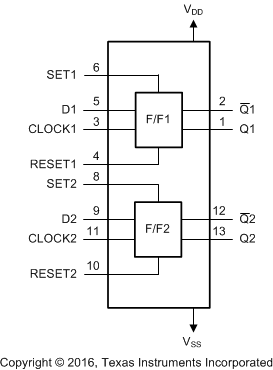
The CD4013B device consists of two identical, independent data-type flip-flops. Each
flip-flop has independent data, set, reset, and clock inputs and Q and Q
outputs. These devices can be used for shift register applications, and, by connecting
Q output to the data input, for counter and toggle applications. The logic
level present at the D input is transferred to the Q output during the positive-going transition of
the clock pulse. Setting or resetting is independent of the clock and is accomplished by a high
level on the set or reset line, respectively.The CD4013B types are supplied in 14-pin dual-in-line plastic packages (E suffix), 14-pin
small-outline packages (M, MT, M96, and NSR suffixes), and 14-pin thin shrink small-outline packages (PW and PWR suffixes).
CD4013BM 数据手册
CD4013BM 电路图