ADS5282IRGCT 供应商
-
ADS5282IRGCT
品牌:TI 封装/批号:原厂原装/22+ -
ADS5282IRGCT
品牌:TI(德州仪器) 封装/批号:VQFN-64/2022+ -
ADS5282IRGCT
品牌:TI 封装/批号:TEJIA/21+
ADS5282IRGCT 属性参数
- 产品培训模块:Data Converter Basics
- 视频文件:ADS528x Low Power 8-Channel, 12-Bit, 50MSPS ADC
- 标准包装:1
- 类别:集成电路 (IC)
- 家庭:数据采集 - 模数转换器
- 系列:-
- 位数:12
- 采样率(每秒):65M
- 数据接口:串行
- 转换器数目:8
- 功率耗散(最大):77mW
- 电压电源:模拟和数字
- 工作温度:-40°C ~ 85°C
- 安装类型:表面贴装
- 封装/外壳:64-VFQFN 裸露焊盘
- 供应商设备封装:64-VQFN 裸露焊盘(9x9)
- 包装:®
- 输入数目和类型:8 个差分,单极
- 配用:296-30655-ND - EVAL MODULE FOR ADS5282
- 其它名称:296-23308-6
产品特性
- Speed and Resolution Grades: ADS5281: 12-bit, 50MSPS ADS5282: 12-bit, 65MSPS
- ADS5281: 12-bit, 50MSPS
- ADS5282: 12-bit, 65MSPS
- Power Dissipation: 48mW/Channel at 30MSPS 55mW/Channel at 40MSPS 64mW/Channel at 50MSPS 77mW/Channel at 65MSPS
- 48mW/Channel at 30MSPS
- 55mW/Channel at 40MSPS
- 64mW/Channel at 50MSPS
- 77mW/Channel at 65MSPS
- 70dBFS SNR at 10MHz IF
- Analog Input Full-Scale Range: 2VPP
- Low-Frequency Noise Suppression Mode
- 6dB Overload Recovery In One Clock
- External and Internal (Trimmed) Reference
- 3.3V Analog Supply, 1.8V Digital Supply
- Single-Ended or Differential Clock: Clock Duty Cycle Correction Circuit (DCC)
- Clock Duty Cycle Correction Circuit (DCC)
- Programmable Digital Gain: 0dB to 12dB
- Serialized DDR LVDS Output
- Programmable LVDS Current Drive, Internal Termination
- Test Patterns for Enabling Output Capture
- Straight Offset Binary or Two’s Complement Output
- Package Options: 9mm × 9mm QFN-64 HTQFP-80 PowerPAD Compatible with ADS527x Family
- 9mm × 9mm QFN-64
- HTQFP-80 PowerPAD Compatible with ADS527x Family
产品概述
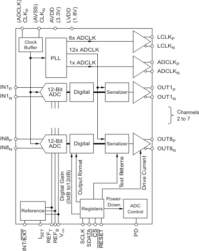
The ADS528x is a family of high-performance, low-power, octal channel analog-to-digital
converters (ADCs). Available in either a 9mm × 9mm QFN package or an HTQFP-80 package, with
serialized low-voltage differential signaling (LVDS) outputs and a wide variety of programmable
features, the ADS528x is highly customizable for a diversity of applications and offers an
unprecedented level of system integration. An application note, XAPP774 (available at www.xilinx.com), describes how to interface the serial LVDS outputs of TI&3146;s ADCs to Xilinx field-programmable gate arrays (FPGAs). The ADS528x family is specified over the industrial temperature range of –40°C to +85°C.
ADS5282IRGCT 数据手册
ADS5282IRGCT 电路图