ADC11C125CISQ 供应商
-
ADC11C125CISQ
品牌:TI 封装/批号:原厂原装/22+ -
ADC11C125CISQ/NOPB
品牌:TI(德州仪器) 封装/批号:48-WQFN/2022+ -
ADC11C125CISQ+
品牌:TI/NS 封装/批号:/21+
ADC11C125CISQ 属性参数
- 制造商:National Semiconductor (TI)
- 转换器数量:1
- ADC 输入端数量:1
- 结构:Pipelined
- 转换速率:125000 KSPs
- 分辨率:11 bit
- 输入类型:Voltage
- 接口类型:Parallel
- 信噪比:65.7 dB
- 电压参考:Internal, External
- Supply Voltage - Max:3.6 V
- Supply Voltage - Min:3 V
- 最大功率耗散:5200 mW
- 最大工作温度:+ 85 C
- 封装 / 箱体:LLP EP
- 封装:Reel
- 最小工作温度:- 40 C
- 工作电源电压:3.3 V
- 工厂包装数量:250
产品特性
- 1.1 GHz Full Power Bandwidth
- Internal Sample-and-Hold Circuit
- Low Power Consumption
- Internal Precision 1.0V Reference
- Single-Ended or Differential Clock Modes
- Clock Duty Cycle Stabilizer
- Dual +3.3V and +1.8V Supply Operation
- Power-Down and Sleep Modes
- Offset Binary or 2's Complement Output Data Format
- Pin-Compatible: ADC14155, ADC12C170, ADC11C170
- 48-pin WQFN Package, (7x7x0.8mm, 0.5mm Pin-Pitch)
- Resolution 11 Bits
- Conversion Rate 125 MSPS
- SNR (fIN = 70 MHz) 65.5 dBFS (typ)
- SFDR (fIN = 70 MHz) 88.2 dBFS (typ)
- ENOB (fIN = 70 MHz) 10.5 bits (typ)
- Full Power Bandwidth 1.1 GHz (typ)
- Power Consumption 608 mW (typ)
产品概述
The ADC11C125 is a high-performance CMOS analog-to-digital converter capable of
converting analog input signals into 11-Bit digital words at rates up to 125 Mega Samples Per
Second (MSPS). This converter uses a differential, pipelined architecture with digital error
correction and an on-chip sample-and-hold circuit to minimize power consumption and the external
component count, while providing excellent dynamic performance. A unique sample-and-hold stage
yields a full-power bandwidth of 1.1 GHz. The ADC11C125 operates from dual +3.3V and +1.8V power
supplies and consumes 608 mW of power at 125 MSPS. The separate +1.8V supply for the digital output interface allows lower power operation
with reduced noise. A power-down feature reduces the power consumption to 5 mW while still allowing
fast wake-up time to full operation. In addition there is a sleep feature which consumes 50 mW of
power and has a faster wake-up time. The differential inputs provide a full scale differential input swing equal to 2 times
the reference voltage. A stable 1.0V internal voltage reference is provided, or the ADC11C125 can
be operated with an external reference.Clock mode (differential versus single-ended) and output data format (offset binary
versus 2's complement) are pin-selectable. A duty cycle stabilizer maintains performance over a
wide range of input clock duty cycles.The ADC11C125 is pin compatible with the ADC12C170 and the ADC14155.It is available in a 48-lead WQFN package and operates over the industrial temperature
range of −40°C to +85°C.
ADC11C125CISQ 数据手册
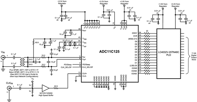
ADC11C125CISQ 电路图