74CB3Q16244DGGRG4 供应商
-
74CB3Q16244DGGRG4
品牌:TI 封装/批号:原厂原装/22+
74CB3Q16244DGGRG4 属性参数
- 标准包装:2,000
- 类别:集成电路 (IC)
- 家庭:逻辑 - 信号开关,多路复用器,解码器
- 系列:74CB
- 类型:FET 总线开关
- 电路:1 x 4:1
- 独立电路:4
- 输出电流高,低:-
- 电压电源:单电源
- 电源电压:2.3 V ~ 3.6 V
- 工作温度:-40°C ~ 85°C
- 安装类型:表面贴装
- 封装/外壳:48-TFSOP(0.240",6.10mm 宽)
- 供应商设备封装:48-TSSOP
- 包装:带卷 (TR)
产品特性
- High-Bandwidth Data Path (Up to 500 MHz)(1)
- 5-V Tolerant I/Os With Device Powered Up or Powered Down
- Low and Flat ON-State Resistance (ron) Characteristics Over Operating Range (ron= 5 Ω Typical)
- Rail-to-Rail Switching on Data I/O Ports 0 to 5-V Switching With 3.3-V VCC 0 to 3.3-V Switching With 2.5-V VCC
- 0 to 5-V Switching With 3.3-V VCC
- 0 to 3.3-V Switching With 2.5-V VCC
- Bidirectional Data Flow With Near-Zero Propagation Delay
- Low Input and Output Capacitance Minimizes Loading and Signal Distortion (Cio(OFF) = 4 pF Typical)
- Fast Switching Frequency (fOE = 20 MHz Maximum)
- Data and Control Inputs Provide Undershoot Clamp Diodes
- Low Power Consumption (ICC = 1 mA Typical)
- VCC Operating Range From 2.3 V to 3.6 V
- Data I/Os Support 0 to 5-V Signaling Levels (0.8 V, 1.2 V, 1.5 V, 1.8 V, 2.5 V, 3.3 V, 5 V)
- Control Inputs Can Be Driven by TTL or 5-V and 3.3-V CMOS Outputs
- Ioff Supports Partial-Power-Down Mode Operation
- Latch-Up Performance Exceeds 100 mA Per JESD 78, Class II
- ESD Performance Tested Per JESD 22 2000-V Human Body Model (A114-B, Class II) 1000-V Charged-Device Model (C101)
- 2000-V Human Body Model (A114-B, Class II)
- 1000-V Charged-Device Model (C101)
- Supports Both Digital and Analog Applications
产品概述
The SN74CB3Q16244 device is a high-bandwidth FET bus switch using a charge pump to
elevate the gate voltage of the pass transistor, providing a low and flat ON-state resistance
(ron). The low and flat ON-state resistance allows for minimal propagation
delay and supports rail-to-rail switching on the data input/output (I/O) ports. The SN74CB3Q16244
device also features low data I/O capacitance to minimize capacitive loading and signal distortion
on the data bus. Specifically designed to support high-bandwidth applications, the SN74CB3Q16244
device provides an optimized interface solution ideally suited for broadband communications,
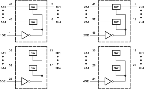
networking, and data-intensive computing systems.The SN74CB3Q16244 device is organized as four 4-bit bus switches with separate
output-enable (1OE, 2OE, 3OE,
4OE) inputs. It can be used as four 4-bit bus switches, two 8-bit bus
switches, or one 16-bit bus switch. When OE is low, the associated 4-bit bus
switch is ON, and the A port is connected to the B port, allowing bidirectional data flow between
ports. When OE is high, the associated 4-bit bus switch is OFF, and a
high-impedance state exists between the A and B ports.This device is fully specified for partial-power-down applications using
Ioff. The Ioff circuitry prevents damaging current
backflow through the device when it is powered down. The device has isolation during power
off.To ensure the high-impedance state during power up or power down,
OE should be tied to VCC through a pullup resistor;
the minimum value of the resistor is determined by the current-sinking capability of the
driver.
74CB3Q16244DGGRG4 电路图